Download presentation
Presentation is loading. Please wait.

1
Dielectric properties of ceramics

2
f Polarization mechanisms
After application of an electric field, the center of gravity of positive and negative charges does not correspond anymore f Electronic Ionic Dipolar Orientation Space charge or diffusional Electronic polarization: deformation of the electronic shell. Atomic or ionic polarization: displacement of negative and positive ions in relation to one another Dipolar and orientation polarization Alignement of dipolar molecules in a liquid Spontaneous alignement of dipoles in a polar solid (ferroelectricity) Ion jump polarization occurs when two or more lattice positions are available for a ion or lattice defect Reorientation of dipolar defects Space charge polarization occurs when charges accumulate at interfaces: composite materials, insulating surface skin, electrode polarization effects
 Ion jump polarization occurs when two or more lattice positions are available for a ion or lattice defect. Reorientation of dipolar defects. Space charge polarization occurs when charges accumulate at interfaces: composite materials, insulating surface skin, electrode polarization effects.")
3
Polarization, capacitance and dielectric constant
h A p Dipoles and surface charges in a polarized dielectric Dipole moment Polarization (dipole moment per unit volume) Dielectric displacement (0 is the vacuum permittivity) Surface charge density For a linear dielectric Capacitance Permittivity Relative permittivity (or dielectric constant) (e is the electric susceptibility)
 Dielectric displacement (0 is the vacuum permittivity) Surface charge density. For a linear dielectric. Capacitance. Permittivity. Relative permittivity (or dielectric constant) (e is the electric susceptibility)")
4
Polarization, capacitance and dielectric constant
Polarizability () (induced dipole moment per unit field) Clausius-Mosotti relationship Electronic polarizabilities are rather independent of crystal environment and high frequency dielectric constant can be predicted is the local field constant More generally “Polarization catastroph” The local field produced by polarization can increase more rapidly than the restoring force thus stabilizing the polarization further possibility of spontaneous polarization (ferroelectric instability) If than for a linear dielectric
 (induced dipole moment per unit field) Clausius-Mosotti relationship. Electronic polarizabilities are rather independent of crystal environment and high frequency dielectric constant can be predicted. is the local field constant. More generally. Polarization catastroph The local field produced by polarization can increase more rapidly than the restoring force thus stabilizing the polarization further possibility of spontaneous polarization (ferroelectric instability) If. than. for a linear dielectric.")
5
Power dissipated per unit time
Dielectric losses Ideal capacitor: 90° phase difference between I and U, no dissipation Voltage Current Angular frequency =2f = 2/T Real capacitor: <90° phase difference between I and U. Ic: charging current (capacitative component) Il: loss current, dissipative comp., power loss Il: in phase with U IC: 90° in advance of U Power dissipated per unit time tan: “dissipation factor” or “loss tangent” rtan: “loss factor” Dissipated power density By analogy with dc current Dielectric or ac conductivity
 Il: loss current, dissipative comp., power loss. Il: in phase with U. IC: 90° in advance of U. Power dissipated per unit time. tan: dissipation factor or loss tangent rtan: loss factor Dissipated power density. By analogy with dc current. Dielectric or ac conductivity.")
6
Complex sinusoidal voltage
Complex permittivity The behaviour of ac circuits can be conveniently analysed using complex quantities Real part 90° in advance Imaginary part Complex sinusoidal voltage Im Re Vacuum capacitor Ic Il Capacitor with a lossy dielectric By analogy with Ohm’s law: I =U/R or J = E

7
Resonance effects in dielectrics
Equation of motion 0: natural vibration frequency : damping factor Q: charge m: mass E: local field Charged particle in a harmonic potential well This behaviour is generally observed for the electronic and ionic polarization processes, where the charges/dipoles move around the equilibrium positions and final polarization is almost instantaneously achieved. Resonant frequencies are of the order of 1013 and 1015 s-1, respectively, and fall in the optical range.

8
Relaxation effects in dielectrics – migration & orientation polarization
Dipolar and space charge polarization is generally accompanied by the diffusional movement of charge and dipoles over several atomic distances and surmounting energy barriers of different high. These polarization processes are relatively slow and strongly temperature dependent (thermally activated). If the transient polarization is described by a simple exponential function, the dipolar relaxation is described by the Debye equation. Reorientation of dipolar defects (defects pairs) Debye relaxation FeTi VO Electrostatic potential in a glass or defective oxide Relaxation time
. If the transient polarization is described by a simple exponential function, the dipolar relaxation is described by the Debye equation. Reorientation of dipolar defects (defects pairs) Debye relaxation. FeTi. VO. Electrostatic potential in a glass or defective oxide. Relaxation time.")
9
’r,s Debye relaxation ’r ’r, ½(’r,s- ’r,) ’’r =1
Frequency dispersion region Debye relaxation Maximum loss occurs when the field frequency is equal to the jump frequency , =1 << r: ions follow the field low losses >> r: ions do not jump low losses Ea takes values typical of ionic conduction processes (0.7 eV), giving a loss peak in the range 103 – 106 Hz.
, giving a loss peak in the range 103 – 106 Hz.")
10
Relaxation effects in dielectrics – migration polarization
Debye relaxation holds when the transient polarization is described by a simple exponential with a single relaxation time. In most materials, including single crystals, a distribution of relaxation times exists and permittivity dispersion is observed over a wider frequency range. This is related to variations of the ionic environment and thermal fluctuations with distance and existence of lattice defects. The extreme case is represented by glasses and amorphous materials. Dielectric dispersion in silicate glasses Dielectric relaxation is better described by the equation (Cole&Cole) which takes into account that the the motion of ions responsible for relaxation can be of cooperative type. = for glasses. = 1: Debye
 which takes into account that the the motion of ions responsible for relaxation can be of cooperative type. = for glasses. = 1: Debye.")
12
Relaxation effects in dielectrics – effect of temperature and frequency
Electronic and ionic polarization resonance occurs at f>1010 Hz which is above the limit of normal uses. The effect of temperature is small. Contribution from ion and defect migration as well as dc conductivity determine a sharp rise of permittivity with increasing temperature and decreasing frequency. Increasing concentration of charge carriers in turn leads to space charge effects. Dielectric constant of single crystal Al2O3 Dielectric constant of soda-lime silica glass

13
Relaxation effects in dielectrics - Space charge polarization
Polycrystalline and polyphase ceramics exhibit interface or space charge polarization (also called Maxwell-Wagner polarization) arising from different conductivity of the various phases. The most important occurrence of this phenomenon is in semiconducting ceramic oxides with resistive (oxidized) grain boundaries (magnetic ferrites, titanates, niobates) , in which the low frequency permittivity can be several orders of magnitude higher than the high frequency dielectric constant and is dominated by the contribution of grain boundaries. d1 d2 (1) (2) Brick-wall model If x = d1/d2 << 1, 1 >> 2 and ’r,1= ’r,2
 arising from different conductivity of the various phases. The most important occurrence of this phenomenon is in semiconducting ceramic oxides with resistive (oxidized) grain boundaries (magnetic ferrites, titanates, niobates) , in which the low frequency permittivity can be several orders of magnitude higher than the high frequency dielectric constant and is dominated by the contribution of grain boundaries. d1. d2. (1) (2) Brick-wall model. If x = d1/d2 << 1, 1 >> 2 and ’r,1= ’r,2.")
14
Special relationships involving permittivity
RF & MW IR UV-Vis At optical frequencies, electronic polarization is the main contribution to permittivity. If n is the index of refraction BaTiO3 single crystal TC =120°C For ferroelectric materials in the paraelectric regime (T > TC) C: Curie constant T0: Curie-Weiss temperature
 C: Curie constant. T0: Curie-Weiss temperature.")
15
Properties and applications of dielectric ceramics of commercial interest

16
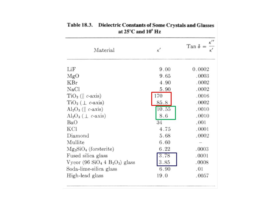
Dielectric losses For alumina ceramics, = ohm cm, ’r = 10, tan = 2x10⁻⁴ at 1 kHz MW region

17
Properties of ceramics with low permittivity and low losses
Typical properties of dielectric ceramics Material Applications Steatite Porcelain insulators Cordierite Applications requiring good thermal shock resistance. Supports for high-power wire-wound resistors. Alumina Best compromise of dielectric losses, high mechanical strength, high thermal conductivity. Reliable metal-ceramic joining technoloy (MolyMn) available. Beryllia Good properties, very high thermal conductivity, expensive and difficult processing. Insulating parts in high-power electromagnetic energy generation (klynstrons and magnetotrons). AlN High thermal conductivity and TEC close to that of silicon. Substrate for power electronic circuits and chips. Glass & glass-ceramics Cheap material and easy processing. Low thermal conductivity
 available. Beryllia. Good properties, very high thermal conductivity, expensive and difficult processing. Insulating parts in high-power electromagnetic energy generation (klynstrons and magnetotrons). AlN. High thermal conductivity and TEC close to that of silicon. Substrate for power electronic circuits and chips. Glass & glass-ceramics. Cheap material and easy processing. Low thermal conductivity.")
19
Properties of ceramics with low permittivity and low losses
Tan of 99.9% alumina ceramics Typical properties of alumina ceramics Spark plugs Insulating parts in high-power electromagnetic generation. Windows for high-power microwave generators. Substrates for electronic circuits. Cheap packaging. 99.9% Al2O3 96% Al2O3 Microstructure of alumina ceramics

20
Electronic substrates and chip packaging

23
Power electronic substrates
The role of the substrate in power electronics is to provide the interconnections to form an electric circuit (like a printed circuit board), and to cool the components. Compared to materials and techniques used in lower power microelectronics, these substrates must carry higher currents and provide a higher voltage isolation (up to several thousand volts). They also must operate over a wide temperature range (up to 150 or 200°C). Direct bonded copper (DBC) substrates are commonly used in power modules, because of their very good thermal conductivity. They are composed of a ceramic tile (commonly alumina) with a sheet of copper bonded to one or both sides by a high-temperature oxidation process. The top copper layer can be preformed prior to firing or chemically etched using printed circuit board technology to form an electrical circuit, while the bottom copper layer is usually kept plain. The substrate is attached to a heat spreader by soldering the bottom copper layer to it. Ceramic materials used in DBC include Al2O3, AlN and BeO.
, and to cool the components. Compared to materials and techniques used in lower power microelectronics, these substrates must carry higher currents and provide a higher voltage isolation (up to several thousand volts). They also must operate over a wide temperature range (up to 150 or 200°C). Direct bonded copper (DBC) substrates are commonly used in power modules, because of their very good thermal conductivity. They are composed of a ceramic tile (commonly alumina) with a sheet of copper bonded to one or both sides by a high-temperature oxidation process. The top copper layer can be preformed prior to firing or chemically etched using printed circuit board technology to form an electrical circuit, while the bottom copper layer is usually kept plain. The substrate is attached to a heat spreader by soldering the bottom copper layer to it. Ceramic materials used in DBC include Al2O3, AlN and BeO.")
24
Dual in-line package (DIP)
Plastic Ceramic (Intel 8080) Ceramic (EPROM) Pin grid array packaging (PGA) Celeron (top) Pentium (bottom) Socket PGA (AMD)
 Ceramic (EPROM) Pin grid array packaging (PGA) Celeron (top) Pentium (bottom) Socket PGA (AMD)")
Similar presentations


 Engr. M. Laiq Ur Rahman>")


