Download presentation
Presentation is loading. Please wait.

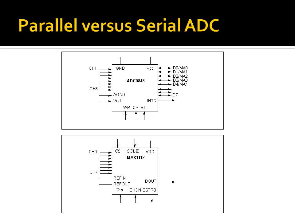
1
Explain the introduction to ADC, ADC characteristics, Programming ADC using PIC18, Introduction to DAC and DAC interfacing with PIC18.

2
Discuss the ADC of the PIC18 Explain the process of data acquisition using ADC Program the PIC18’s ADC in assembly Describe the basic operation of DAC Interface a DAC chip to the PIC18

3
Digital Computer: Binary (discrete) values Physical World: Analog (continuous) values Example: Temperature, Humidity, Pressure Output: Voltage or Current Microcontroller? -----> Digital Therefore, ADC is needed to translate (convert) the analog signals to digital numbers
 the analog signals to digital numbers.")
4
Microcontroller Connection to Sensor via ADC

5
n-bitNo. of stepsStep size (mV) 82 8 = 2565/256 = 19.53 102 10 = 10245/1024 = 4.88 122 12 = 40965/4096 = 1.2 Assuming V REF = 5V * Step Size (Resolution): is the smallest change that can be discerned by an ADC
 82 8 = 2565/256 = = 10245/1024 = = 40965/4096 = 1.2 Assuming V REF = 5V * Step Size (Resolution): is the smallest change that can be discerned by an ADC.")
6
V ref : Input voltage used for the reference voltage The voltage connected to this pin, with the resolution of the ADC chip, dictate the step size Example: If we need the analog input to be 0 to 4 volts, V ref is connected to 4 volts Digital data output: 8-bit (D0-D7), 10-bit (D0- D9)
, 10-bit (D0- D9)")
7
V ref (V)V in (V)Step size (mV) 5.000 to 55/1024 = 4.88 4.0960 to 4.0964.096/1024 = 4 3.00 to 33/1024 = 2.93 2.560 to 2.562.56/1024 = 2.5 2.0480 to 2.0482.048/1024 = 2 V ref Relation to Vin Range for an 10-bit ADC
V in (V)Step size (mV) to 55/1024 = to /1024 = to 33/1024 = to /1024 = to /1024 = 2 V ref Relation to Vin Range for an 10-bit ADC")
8
D out = V in / Step Size Digital data output (in decimal): 8-bit (D0-D7)= 256 10-bit (D0-D9) = 1024 Analog Input Voltage Example: V ref = 2.56, V in = 1.7V. Calculate the Do-D9 output? Solution: Step Size = 2.56/1024 = 2.5mV Dout = 1.7/2.5mV = 680 (Decimal) D0-D9 = 1010101000
 D0-D9 =")
11
It has 11 analog input channels (AN0 – AN10) 10-bit ADC Converted values are stored in ADRESH:ADRESL registers
 10-bit ADC Converted values are stored in ADRESH:ADRESL registers")
12
A/D Control Register 0 (ADCON0) Controls the operation of the A/D module A/D Control Register 1 (ADCON1) Configures the functions of the port pins A/D Control Register 2 (ADCON2) Configures the A/D clock source, programmed acquisition time and justification
 Controls the operation of the A/D module A/D Control Register 1 (ADCON1) Configures the functions of the port pins A/D Control Register 2 (ADCON2) Configures the A/D clock source, programmed acquisition time and justification")
13
Different from the Book! Example: ADCON0 = 00101001

14
* Different from the Book!

15
Example: ADCON1 = 00001110 * Different from the Book!

16
Example: ADCON2 = 10000110

17
ADFM Bit and ADRESx Registers

18
For a PIC18-based system, we have V ref = V dd = 5V. Find a) The step size and b) The ADCON1 value if we need 3 channels. a)The step size = 5/1024 = 4,8mV b)ADCON1 = 00001100
 The step size and b) The ADCON1 value if we need 3 channels. a)The step size = 5/1024 = 4,8mV b)ADCON1 =")
19
Define in term of Tad (Conversion time per bit) To calculate: F OSC /2, F OSC /4, F OSC /8, F OSC /16, F OSC /32 or F OSC /64
 To calculate: F OSC /2, F OSC /4, F OSC /8, F OSC /16, F OSC /32 or F OSC /64")
20
TURN ON the ADC module (BSF ADCON0, ADON) Make the ADC channel pin as input pin Select voltage reference and ADC channel Select the conversion speed Wait for the required acquisition time Activate the start conversion bit of GO/DONE Wait for the conversion to be completed by pooling the end-of-conversion GO/DONE bit After the GO/DONE bit has gone LOW, read the ADRESL and ADRESH register
 Make the ADC channel pin as input pin Select voltage reference and ADC channel Select the conversion speed Wait for the required acquisition time Activate the start conversion bit of GO/DONE Wait for the conversion to be completed by pooling the end-of-conversion GO/DONE bit After the GO/DONE bit has gone LOW, read the ADRESL and ADRESH register")
21
ORG0000H CLRFTRISC CLRF TRISD BSFTRISA, 0 MOVLW0x00 MOVWFADCON0 MOVLW0x0E MOVWFADCON1 MOVLW0xBE MOVWFADCON2 OV ERCALLDELAY BSFADCON0, GO BACKBTFSADCON0, GONE BRABACK MOVFFADRESL, PORTC MOVFFADRESH, PORTD CALLQSEC_DELAY BRAOVER END

22
InterruptFlag BitRegisterEnable BitRegister ADIF (ADC)ADIFPIR1ADIEPIE1 ADC Interrupt Flag Bits and Associated Registers * Please see Program 13-2 page 514
ADIFPIR1ADIEPIE1 ADC Interrupt Flag Bits and Associated Registers * Please see Program 13-2 page 514")
23
Covert digital pulses to analog pulses DAC0808 chip: Use R/2R method, 8-bit DAC Block Diagram

25
The digital inputs are converted to current (I out ) Connecting a resistor to the I out pin, we convert the result to voltage I out = I ref (D7/2 + D6/4 + D5/8 + D4/16 + D3/32 + D2/64 + D1/128 + D0/256) I ref = Generally set to 2.0mA This will course inaccuracy because the Resistance will affect the reading
 Connecting a resistor to the I out pin, we convert the result to voltage I out = I ref (D7/2 + D6/4 + D5/8 + D4/16 + D3/32 + D2/64 + D1/128 + D0/256) I ref = Generally set to 2.0mA This will course inaccuracy because the Resistance will affect the reading")
26
Example: Binary input: 10011001 I out = 2mA (153/256) = 1.195mA and V out = 1.195mA x 5K = 5.975V
 = 1.195mA and V out = 1.195mA x 5K = 5.975V")
27
Gas Sensor Temperature Sensor Humidity Sensor Sonar Sensor

28
Characteristic: 1)Precision integrated-circuit 2)Output voltage is linearly proportional to the Celcius 3)Requires no external calibration (Internally calibration) 4)Output: 10mV for each degree
Precision integrated-circuit 2)Output voltage is linearly proportional to the Celcius 3)Requires no external calibration (Internally calibration) 4)Output: 10mV for each degree")
29
10mV = 1 degree (Minimum) 20mV = 2 degree 30mV = 3 degree. 1000mV = 100 degree (Maximum) Vr ef = ??? 5V 1.024 Step Size = 4.8mV Step Size = 1mV Vin (max) = 5V Vin (max) = 1.024V Which one suitable? How to set V ref ??
 Vr ef = . 5V Step Size = 4.8mV Step Size = 1mV Vin (max) = 5V Vin (max) = 1.024V Which one suitable. How to set V ref .")
30
To overcome any fluctuations in power supply. * Please see Program 13-4 page 524

31
“Things are only impossible until they're not”

Similar presentations


 And>")
 & Digital-to-Analog Conversion (DAC) Read. Homework #13 and Lab #13 due next week. >")


