Download presentation
Presentation is loading. Please wait.

1
Voltage-Series Feedback
Two examples of the voltage-series topology are considered in this section: (a) The FET common drain amplifier (source follower), and (b) The bipolar transistor common-collector amplifier (emitter follower). The FET Source Follower The circuit is given in Fig a. For AC analysis, all capacitors (dc blocking and bypass) are considered short circuited and the biasing voltages should be grounded as shown in Fig Prepared by Dr. M. A. Mannan
 The FET common drain amplifier (source follower), and. (b) The bipolar transistor common-collector amplifier (emitter follower). The FET Source Follower. The circuit is given in Fig a. For AC analysis, all capacitors (dc blocking and bypass) are considered short circuited and the biasing voltages should be grounded as shown in Fig Prepared by Dr. M. A. Mannan.")
2
In Fig. 13-12.1 the terminals G and S are used for input and D and S are used for output.
The feedback is the voltage Vf across R, and the sampled signal is the output voltage Vo across R. Hence, this is the case of voltage-series feedback. We must now draw the basic amplifier without feedback where all grounds are eliminated. To find the input circuit, set Vo=0 (the output loop is shorted) as shown in Fig (a). Hence Vs appears directly between G and S as shown in Fig (b).
 as shown in Fig (a). Hence Vs appears directly between G and S as shown in Fig (b).")
3
Hence R appears only in the output loop.
To find the output circuit, set Ii=0 (the input loop is opened) shown in Fig (a). Finally, we obtained Fig (b) by adding Fig (b) and Fig (b).
 shown in Fig (a). Finally, we obtained Fig (b) by adding Fig (b) and Fig (b).")
4
If the FET is replaced by its low-frequency model, the result is Fig
If the FET is replaced by its low-frequency model, the result is Fig (c). From the figure Vf and Vo are equal, and b= Vf / Vo =1. This topology stabilizes voltage gain. AV is calculated by inspection of fig c. Since without feedback Vi=Vs, then
. From the figure Vf and Vo are equal, and b= Vf / Vo =1. This topology stabilizes voltage gain. AV is calculated by inspection of fig c. Since without feedback Vi=Vs, then.")
5
The input impedance of an FET is infinite, Ri=, and hence Rif=RiD=.
We are interested in finding the output resistance seen looking into the FET source S. Then, Ro=rd. Hence R is considered an external load RL. Thus RL= R. Then Since three assumptions are satisfied, the above results are exact for voltage-series feedback topology.

6
The Emitter Follower The circuit is given in Fig. 13-12a.
Equivalent circuit for ac analysis is shown in Fig In Fig the terminals B and E are used for input and C and E are used for output. The feedback is the voltage Vf across Re, and the sampled signal is the output voltage Vo across Re. Hence, this is the case of voltage-series feedback. We must now draw the basic amplifier without feedback where all grounds are eliminated.

7
To find the input circuit, set Vo=0 (the output loop is shorted) as shown in Fig. 13-13.2(a).
Hence Vs in series with Rs appears between B and E. To find the output circuit, set Ii=0 (the input loop is opened) shown in Fig (a). Hence R appears only in the output loop.
 shown in Fig (a). Hence R appears only in the output loop.")
8
Finally, we obtained Fig. 13-13(b) by adding Fig. 13-13. 2 (b) and Fig
Finally, we obtained Fig (b) by adding Fig (b) and Fig (b). If the transistor is replaced by its low-frequency approximate model, the results is Fig (c).
 by adding Fig (b) and Fig (b). If the transistor is replaced by its low-frequency approximate model, the results is Fig (c).")
9
From this figure Vo=Vf and b=Vf/Vo=1.
This topology stabilizes the voltage gain. AV is calculated by inspection of Fig c. Since Rs is considered as part of the amplifier then Vi=Vs, and For hfeRe>>Rs+hie, AVf1, as it should be for an emitter follower. The input resistance without feedback is Ri=Rs+hie from Fig c.

10
We are interested in the resistance seen looking into the emitter.
Hence Re is considered as an external load i.e. RL=Re. From Fig c, we are looking into a current source Ro= and Thus for this voltage-series topology, we get The indeterminacy in Eq. (13-48) may be resolved by first evaluating Rof’ =and then going to the limit Re. Thus, since Ro’ =Re.
 may be resolved by first evaluating Rof’ =and then going to the limit Re. Thus, since Ro’ =Re.")
11
It is seen form the above equations that the feedback desensitizes voltage gain with respect to changes in hfe and that it increases the input resistance and decreases the output resistance. The forgoing expressions for AVf, Rif and Rof are based on the assumption of zero forward transmission through the feedback network. Since there is such forward transmission because the input current passes through Re in fig a, these expressions are only approximately true.

12
A Voltage-Series Feedback Pair
Fig shows two cascaded stages whose voltage gains are AV1, and AV2. The output of the second stage is returned through the feedback network R1R2 in opposition to the input signal Vs. Clearly, then this is a case of voltage-series negative feedback. The first basic assumption is not strictly satisfied for the circuit of Fig a because I’ represents transmission through the feedback network from input to the output. We shall neglect I’ compared with I on the realistic assumption that the current gain of the second stage is much larger than unity.

13
The input of the basic circuit without feedback is found by setting Vo=0 and hence R2 appears in parallel with R1 as shown in Fig (a) and (b). The output of the basic amplifier without feedback is found by opening the input loop (set I’=0) and hence R1 is placed in series with R2 as shown in Fig (a) and (b).
 and hence R1 is placed in series with R2 as shown in Fig (a) and (b).")
14
Finally, we obtained Fig. 13-14(b) by adding Fig. 13-14. 2 (b) and Fig
Finally, we obtained Fig (b) by adding Fig (b) and Fig (b). According to Fig b, the series feedback voltage Vf across R1 in the output circuit. Thus,
 by adding Fig (b) and Fig (b). According to Fig b, the series feedback voltage Vf across R1 in the output circuit. Thus,")
15
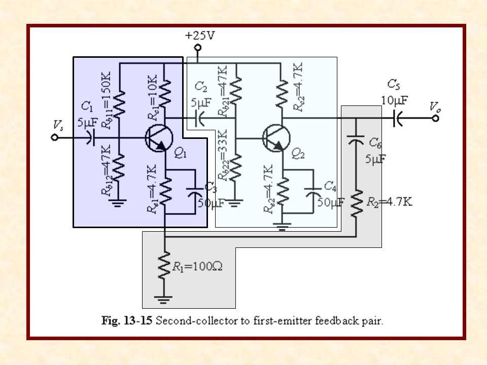
Second-Collector to First-Emitter Feedback Pair
The circuit of Fig shows a two-stage amplifier which makes use of voltage-series feedback by connecting the second collector to the first emitter through the voltage divider R1R2. Capacitors C1, C2 (coupling), C5, and C6 are dc blocking capacitors, and capacitors C3 and C4 are bypass capacitors for the emitter bias resistors. All these capacitances represent negligible reactances (short-circuited) at the frequencies of operation of this circuit.
, C5, and C6 are dc blocking capacitors, and capacitors C3 and C4 are bypass capacitors for the emitter bias resistors. All these capacitances represent negligible reactances (short-circuited) at the frequencies of operation of this circuit.")
17
(i) Fig. 13-15 shows two BJT common-emitter cascaded stages.
Example: (i) Identify the topology of the feed back amplifier of Fig , and (ii) Calculate AVf, Rof, and Rif for the amplifier of Fig Assume Rs=0, hfe=1.1K, hre=hoe=0, and identical transistors. Solution: (i) Fig shows two BJT common-emitter cascaded stages. The output of the second stage is returned through the feedback network R1R2 in opposition to the input signal Vs. The feedback signal is voltage. Thus, this is a case of voltage-series negative feedback. (ii) first calculate the overall voltage gain without feedback from AV= AV1AV2.
 Identify the topology of the feed back amplifier of Fig , and (ii) Calculate AVf, Rof, and Rif for the amplifier of Fig Assume Rs=0, hfe=1.1K, hre=hoe=0, and identical transistors. Solution: (i) Fig shows two BJT common-emitter cascaded stages. The output of the second stage is returned through the feedback network R1R2 in opposition to the input signal Vs. The feedback signal is voltage. Thus, this is a case of voltage-series negative feedback. (ii) first calculate the overall voltage gain without feedback from AV= AV1AV2.")
18
The effective load RL1’ of transistor Q1 is
The effective emitter impedance Re1 of transistor Q1 is The effective emitter impedance Re2 of transistor Q2 is zero (i.e. Re2=0). Generally, the gain of a common-emitter amplifier is as follows:
. Generally, the gain of a common-emitter amplifier is as follows:")
19
Thus, the voltage gain for the first stage amplifier of Q1 can be obtained as follows:
Similarly, the voltage gain for the first stage amplifier of Q2 can be obtained as follows: Hence, the voltage gain AV of the two stages in cascade without feedback is The feedback factor of Fig is as follows: Thus:

20
The return difference and gain with feedback is obtained as follows:
The input resistance without external feedback is: Hence, the input resistance with feedback is obtained as follows: The output resistance without external feedback is: Hence, the output resistance with feedback is obtained as follows:

21
Current-Series Feedback
Transistor Configuration The circuit of transistor configuration as current series feedback is given in Fig a. The feedback signal is the voltage Vf across Re and the sampled signal is the load current Io. Hence, this is a case of current-series feedback. Although Io is proportional to Vo, it is not correct to conclude that this is a voltage-series feedback. Thus, if the output signal is taken as the voltage Vo, then Since b is now a function of the load RL, the third basic assumption given in section 13-3 is violated.

22
The input circuit of the amplifier without feedback is obtained by opening the output loop (Io=0).
Hence Re must appear in the input side. Similarly, the output circuit is obtained by opening the input loop (Ii=0), and this places Re also in the output side. The resulting equivalent circuit is given in Fig b. The circuit of Fig b represents the basic amplifier without feedback, but tasking the loading of the b network into account.
, and this places Re also in the output side. The resulting equivalent circuit is given in Fig b. The circuit of Fig b represents the basic amplifier without feedback, but tasking the loading of the b network into account.")
23
If the transistor of Fig
If the transistor of Fig (b) is replaced by its low-frequency approximate model, the results is Fig (c). Since the feedback voltage Vf appears across Re in the output circuit, then from Fig c Since the input signal Vi without feedback is the Vs of the Fig c, then
 is replaced by its low-frequency approximate model, the results is Fig (c). Since the feedback voltage Vf appears across Re in the output circuit, then from Fig c. Since the input signal Vi without feedback is the Vs of the Fig c, then.")
24
If (1+hfe)Re>>Rs+hie, and since hfe>>1, then GMf-1/Re, in agreement with GMf1/b. If Re is stable resistor, the transconductance gain with feedback is stabilized (desensitized). The load current is given by Under the conditions (1+hfe)Re>>Rs+hie and hfe>>1, the load current is directly proportional to the input voltage, and this current depends only upon Re, and the not upon any other circuit or transistor parameter.
Re>>Rs+hie and hfe>>1, the load current is directly proportional to the input voltage, and this current depends only upon Re, and the not upon any other circuit or transistor parameter.")
25
The voltage gain is given by
Subject to the conditions (1+hfe)Re>>Rs+hie and hfe>>1, and the voltage gain is stable if RL and Re are stable resistors. From Fig c, we see that Ri=Rs+hie+Re, hence Since Ro=, then Rof=Ro(1+bGm)= . Hence
Re>>Rs+hie and hfe>>1, and the voltage gain is stable if RL and Re are stable resistors. From Fig c, we see that Ri=Rs+hie+Re, hence. Since Ro=, then Rof=Ro(1+bGm)= . Hence.")
26
a. GMf= GM/D=-1 mA/V then GM= -50 mA/V.
Example: The circuit of Fig a is to have an overall transconductance gain of –1mA/V, a voltage gain of –4, and a desensitivity of 50. If Rs=1 K, hfe=150, and rbb’ is negligible, find (a) Re, (b) RL, (c) Rif, and (d) the quiescent collector current Ic at room temperature. Solution: a. GMf= GM/D=-1 mA/V then GM= -50 mA/V. Since b=-Re, then D=1+bGM=1+50Re= 50; Or Re =0.98K 1 K. b. AVf=GMfRL or RL=AVf/GMf= (-4)/(-1)= 4 K.
 Re, (b) RL, (c) Rif, and (d) the quiescent collector current Ic at room temperature. Solution: a. GMf= GM/D=-1 mA/V then GM= -50 mA/V. Since b=-Re, then D=1+bGM=1+50Re= 50; Or Re =0.98K 1 K. b. AVf=GMfRL or RL=AVf/GMf= (-4)/(-1)= 4 K.")
27
c. From Eq. (13-53) GM=-50=(-hfe)/(Rs+hie+Re)=(-150)/(1+hie+1) then hie=1 K. Ri= Rs+hie+Re= 3 K Rif= RiD= (3)(50)=150K d. From Eqs. (11-9) and (11-6) hie=rbb’+rb’e(hfe)/(gm)=(hfeVT/IC) then IC=(hfeVT/hie)=(150)(0.026)/91)=3.9mA.
 and (11-6) hie=rbb’+rb’e(hfe)/(gm)=(hfeVT/IC) then IC=(hfeVT/hie)=(150)(0.026)/91)=3.9mA.")
28
FET Configuration The circuit of FET CS Stage with a source resistor R as current series feedback is given in Fig a. The circuit of Fig a is analogous for the transistor (Fig a) CE stage with an emitter resistor Re. Proceeding as we did for the transistor amplifier, we obtain the circuit of Fig b. Replacing the FET by its low-frequency model results in Fig c.
 CE stage with an emitter resistor Re. Proceeding as we did for the transistor amplifier, we obtain the circuit of Fig b. Replacing the FET by its low-frequency model results in Fig c.")
29
To calculate Rof we need Gm

30
The output resistance without considering load RL is

31
Current-Shunt Feedback
Figure shows two transistors in cascade with feedback from the second emitter to the first base through the resistor R’. The voltage Vi2 is much larger than Vi1 because of the voltage of Q1. Also, Vi2 is 180o out of phase with Vi1. Because of emitter-follower action, Ve2 is only slightly smaller than Vi2, and these voltages are in phase. Hence Ve2 is larger in magnitude than Vi1 and is 180o out of phase with Vi1. If the input signal increases so that Is’ increases, If also increases, and Ii=Is’-If is smaller than it would be if there is no feedback.

32
This action is characteristic of negative feedback.
Thus the circuit of Fig acts as a negative feedback. Since Ve2>>Vi1, and neglecting the base current of Q2 compared with the collector current, Since the feedback current is proportional to the output current, this circuit of Fig acts as a current shunt feedback amplifier.

33
If Re, R’, Rc2, and Rs are stable elements, then AVf is stable.
The current gain with feedback of this circuit is: So, AIf is stable (desensitized) provided that R’ and Re are stable resistances. The voltage gain with feedback of this circuit is: If Re, R’, Rc2, and Rs are stable elements, then AVf is stable.
 provided that R’ and Re are stable resistances. The voltage gain with feedback of this circuit is: If Re, R’, Rc2, and Rs are stable elements, then AVf is stable.")
34
Amplifier Without Feedback of Fig. 13-18
The input circuit of the amplifier without feedback is obtained by opening the output loop at the emitter of Q2. This places R’ in series with Re from base to emitter Q1. The output circuit is found by shorting the input node (the base of Q1). This places R’ in parallel with Re. The resultant equivalent circuit is given in Fig Since the feedback signal is a current, the source is represented by a Norton’s equivalent circuit with Is=Vs/Rs.
. This places R’ in parallel with Re. The resultant equivalent circuit is given in Fig Since the feedback signal is a current, the source is represented by a Norton’s equivalent circuit with Is=Vs/Rs.")
35
Voltage-Shunt Feedback
Figure 13-20a shows a common-emitter stage with a resistor R’ connected from the output to the input. In the circuit of Fig a, the output voltage Vo is much greater than the input voltage Vi and is 180o out of phase with Vi. Hence Since the feedback current is proportional to the output voltage, this circuit acts as a voltage-shunt feedback amplifier. The transresistance with feedback is obtained as follows:

36
The transresistance equals the negative of the feedback resistance from output to input of the transistor and is stable if R’ is a stable resistance. If we assume that Rif’=0, then the voltage gain with feedback is If R’ and Rs are stable elements, then AVf is stable.

37
Amplifier Without Feedback of Fig. 13-20(a)
The input circuit of the amplifier without feedback is obtained by shorting the output node (Vo=0). This places R’ from base to emitter of the transistor. The output circuit is found by shorting the input node (Vi=0), thus connecting R’ from collector to emitter. The resultant equivalent circuit is given in Fig b. Since the feedback signal is a current, the source is represented by a Norton’s equivalent with Is=Vs/Rs. The feedback signal is the current If in the resistor R’ which is in the output circuit. From Fig b
. This places R’ from base to emitter of the transistor. The output circuit is found by shorting the input node (Vi=0), thus connecting R’ from collector to emitter. The resultant equivalent circuit is given in Fig b. Since the feedback signal is a current, the source is represented by a Norton’s equivalent with Is=Vs/Rs. The feedback signal is the current If in the resistor R’ which is in the output circuit. From Fig b.")
38
If the amplifier is deactivated by reducing hfe to zero, a current If passes through the b network (the resistor R’) from input to output. This current is given by The output current Io with amplifier activated is Hence the condition that the forward transmission through the feedback network can be neglected is Io>>If, or Since the voltage gain is at least unity, this inequality is easily satisfied by selecting Rs+R’>>Rc.

Similar presentations


 transistors start to manifest.>")

 Amplifier *DC biasing ● Calculate I C, I B, V CE ● Determine related small signal.>")


