Download presentation
Presentation is loading. Please wait.

1
PREZENTACIJA OPREME Institut za nuklearne nauke “Vinča” Laboratorija za atomsku fiziku Nataša Bibić

2
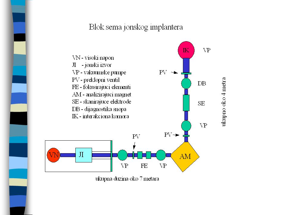
Skanirajući elektronski mikroskop Philips SEM 501 Transmisioni elektronski mikroskop Philips EM 400 Van de Graaff akcelerator Proizvodjač je High Voltage Engineering Corp. Cambridge-Massachusetts. Koristi Van de Graaff-ov generator 500kV Jonski implanter Visoko-naponski terminal ide od minimalnog napona 30-50 kV do maksimalnog od 500 kV.

3
TEM i SEM Donacija King’ College London Van de Graaff akcelerator 500kV Jonski implanter Donacija Univerzitet Surrey, UK Februar Oktobar 2004.god Sredstva MNZŽS

4
History: Alhazen First record of using glass lens for magnification was by an Arabian from what is now known as Iran, Alhazen, in the 10 and 11th century. He contradicted Ptolemy's and Euclid's theory of vision that objects are seen by rays of light emanating from the eyes; according to him the rays originate in the object of vision and not in the eye. Because of his extensive research on vision, he has been considered by many as the father of modern optics.

5
15th century on - Studies done with glass magnifiers to study objects in detail mostly as a curiosity by non- scientists - Antonie van Leeuwenhoek (linen draper) described three shapes of bacterial cells using his simple, single lens microscope (glass bead in metal holder).
 described three shapes of bacterial cells using his simple, single lens microscope (glass bead in metal holder).")
8
Max Knoll1935 - Max Knoll demonstrates the theory of the scanning electron microscope Knoll and Ruska 1986 Nobel Prize winners von Ardenne Ruskavon Borries 1939 - Ruska and von Borries, working for Siemens produce the first commercially available EM von Ardenne 1938 - First scanning electron microscope produced by von Ardenne

9
The greater the accelerating voltage the shorter the voltage the shorter the Therefore, a 50,000 volt (50 kV) electron has a wavelength of 0.0055nm and a 1MeV electron has a wavelength of 0.00123nm! Resolution ½ Resolution is limited to approx. 1/2 the wavelength of illuminating source.

12
1 MeV 200 kV 100kV

13
SEM TEM

14
SEM

15
TEM

16
Electron scattering from specimen Resolution depends on spot size Typically a few nanometers Topographic scan range: order of mm X mm X rays: elemental analysis

17
Electron Microscopy is usefully because we can resolve very small things. SEM works with reflected electrons yielding surface information. TEM works with transmitted electrons yielding information inside your sample.

18
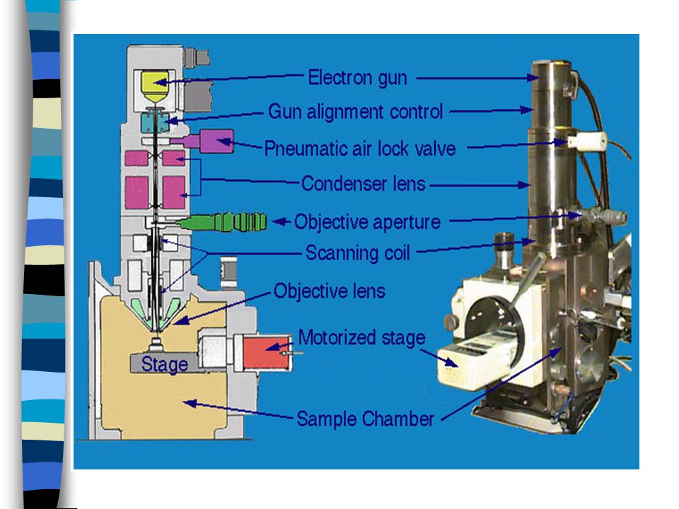
Scanning Electron Microscope

22
SEMs are patterned after Reflecting Light Microscopes and yield similar information: Topography The surface features of an object or "how it looks", its texture; detectable features limited to a few nanometers Morphology The shape, size and arrangement of the particles making up the object that are lying on the surface of the sample or have been exposed by grinding or chemical etching; detectable features limited to a few nanometers Composition The elements and compounds the sample is composed of and their relative ratios, in areas ~ 1 micrometer in diameter Crystallographic Information The arrangement of atoms in the specimen and their degree of order; only useful on single-crystal particles >20 micrometers

23
Philips SEM 501 Laboratorija za atomsku fiziku

24
Transmission Electron Microscopes: Widely used in materials science and biological research Capable of magnifying over a extremely wide range (~100 to >1,000,000 x) Excellent spatial resolution (better than 1 nm) Easy to use and very reliable
 Excellent spatial resolution (better than 1 nm) Easy to use and very reliable")
25
Disadvantages of TEMs: Very expensive to own and operate. Specimen preparation can be time consuming and technically difficult. Specimen is usually chemically fixed and epoxy embedded. Specimen must be sliced into very, very thin sections. *the inside of an electron microscope is a very hostile environment. It is under high vacuum with zero humidity. Also, in the time it takes to make an average 2 sec exposure of your specimen with an 80 KeV beam, the amount of energy the specimen receives is about 5 x10 9 rads, which is approximately equivalent to the radiation delivered from a 10 megatonHydrogen bomb exploding 30 meters away!

26
TEMs are patterned after Transmission Light Microscopes and will yield similar information. Morphology The size, shape and arrangement of the particles which make up the specimen as well as their relationship to each other on the scale of atomic diameters. Crystallographic Information The arrangement of atoms in the specimen and their degree of order, detection of atomic-scale defects in areas a few nanometers in diameter Compositional Information (if so equipped) The elements and compounds the sample is composed of and their relative ratios, in areas a few nanometers in diameter
 The elements and compounds the sample is composed of and their relative ratios, in areas a few nanometers in diameter.")
27
100 keV e - =0.072 angstr. HRTEM sp. res. 0.2 nm

28
A simplified ray diagram of a TEM consists of an electron source, condenser lens with aperture, specimen, objective lens with aperture, projector lens and fluorescent screen.

29
Transmission Electron Microscope Basic premise of a TEM is to project a magnified image of the specimen onto a fluorescent screen where it can be viewed by the operator. The image itself is the result of beam electrons that are scattered by the specimen vs. those that are not.

30
In actuality a modern TEM consists of many more components including a dual condenser system, stigmators, deflector coils, and a combination intermediate and dual projector lens.

31
Total magnification in the TEM is a combination of the magnification from the objective lens times the magnification of the intermediate lens times the magnification of the projector lens. Each of which is capable of approximately 100X. M ob X M int X M proj = Total Mag

34
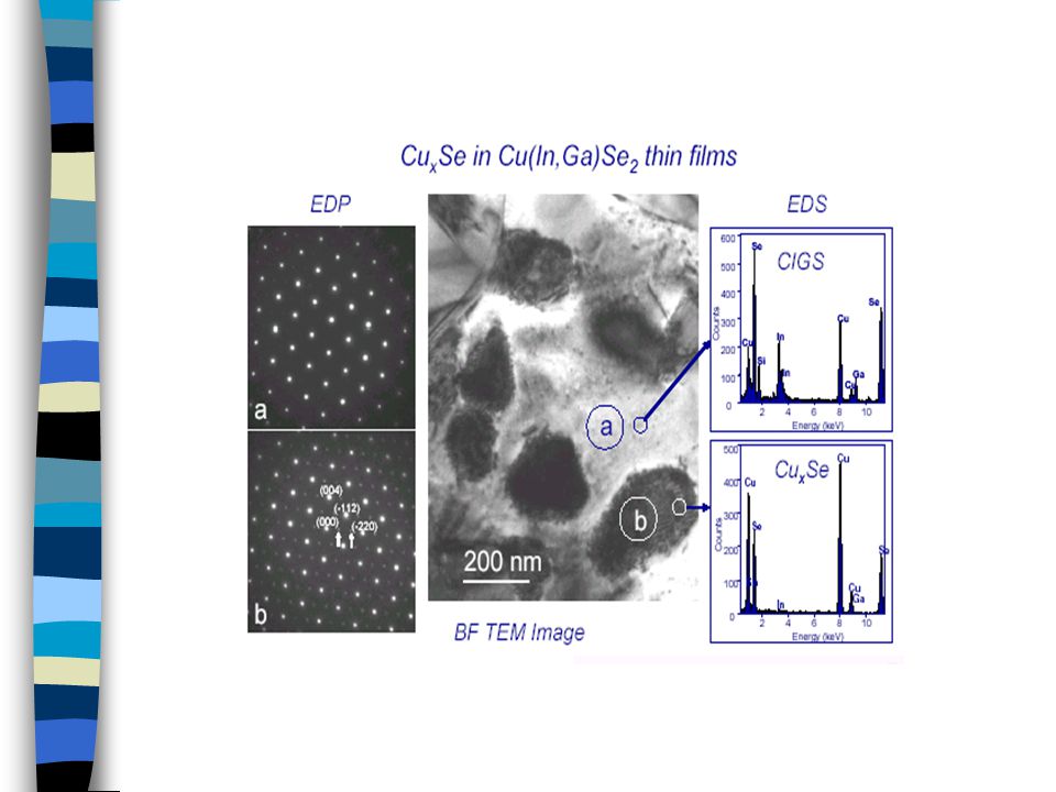
Growth of b-FeSi2 films via noble-gas ion-beam mixing of Fe/Si bilayers

36
Amorphous-iron disilicide: A promising semiconductor

38
TEM IMAGES

39
Philips EM 400 Laboratorija za atomsku fiziku

40
Korisnici Lokacija, Zaduženje Iskorišćenost Laboratorija 040 N. Bibić M.Popović M.Novaković S. Petrović Laboratorije 040, 020, 030, 050,170 Univerzitet u Novom Sadu TEM i SEM Period od 1 godine i značajna iskorištenost

41
SAMPLE PREPARATION Dodatna oprema za pripremu uzoraka Potrebe

42
Van de Graaff akcelerator High Voltage Engineering Corp. Cambridge-Massachusetts. Van de Graaff-ov generator 500kV Jonski implanter Visoko-naponski terminal od minimalnog napona 30-50 kV do maksimalnog od 500 kV.

43
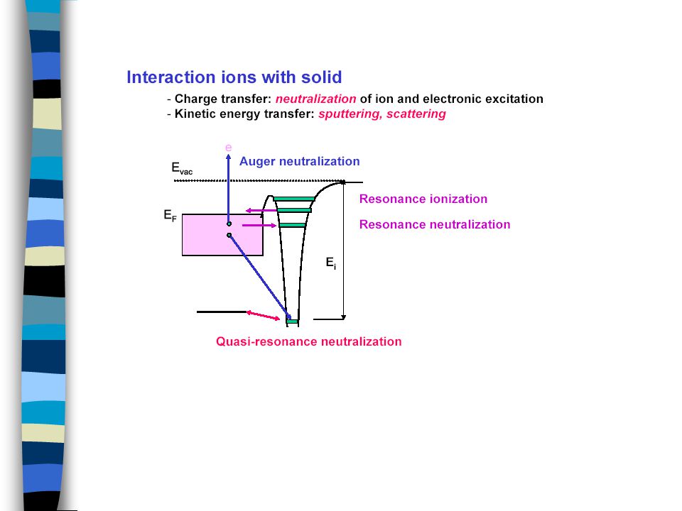
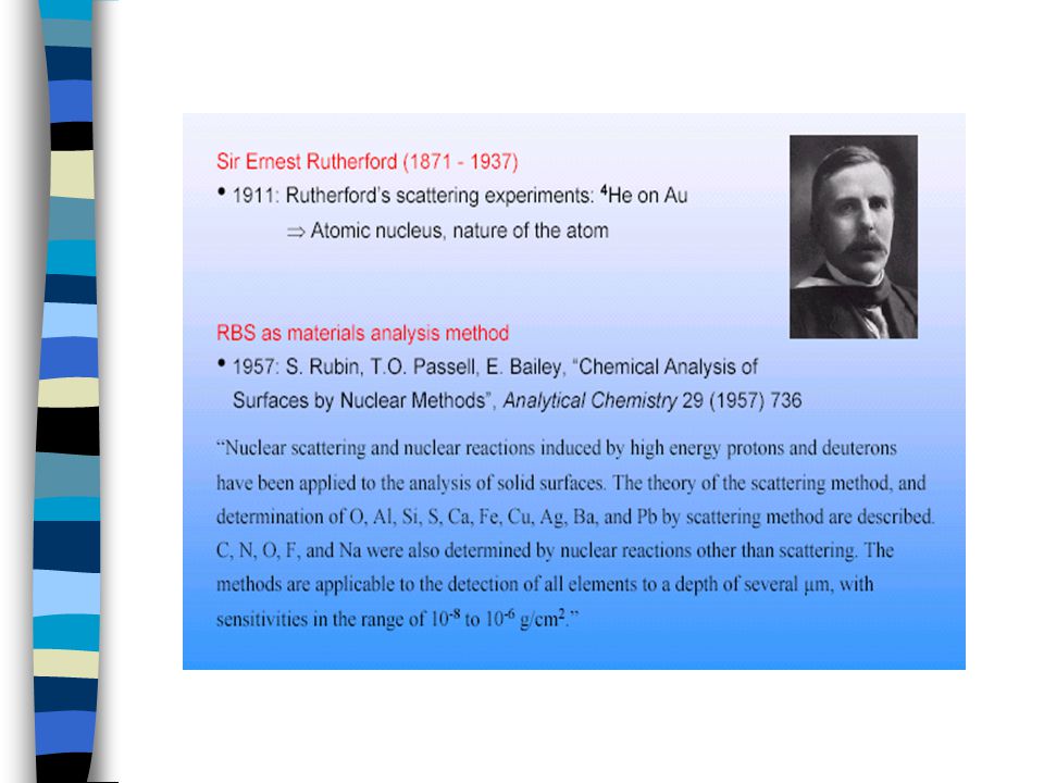
THE ATOMIC ELECTRONS and/or THE ATOMIC NUCLEI In its passage through matter, an ion may interact with

46
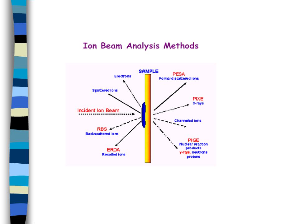
Principles of ion beam analysis

51
RBS In RBS, a beam of mono-energetic (1-2 MeV) collimated light ions (H +, He + ) impinges (usually at normal incidence) on a target and the number and energy of particles that are scattered backwards at a certain angle are monitored to obtain information about the composition of the target (host species and impurities) as a function of depth.
 collimated light ions (H +, He + ) impinges (usually at normal incidence) on a target and the number and energy of particles that are scattered backwards at a certain angle are monitored to obtain information about the composition of the target (host species and impurities) as a function of depth.")
57
Kinematic factor, Mass identification Energy loss, Depth scale Scattering cross sections, Composition, (quantitative) RBS
 RBS")
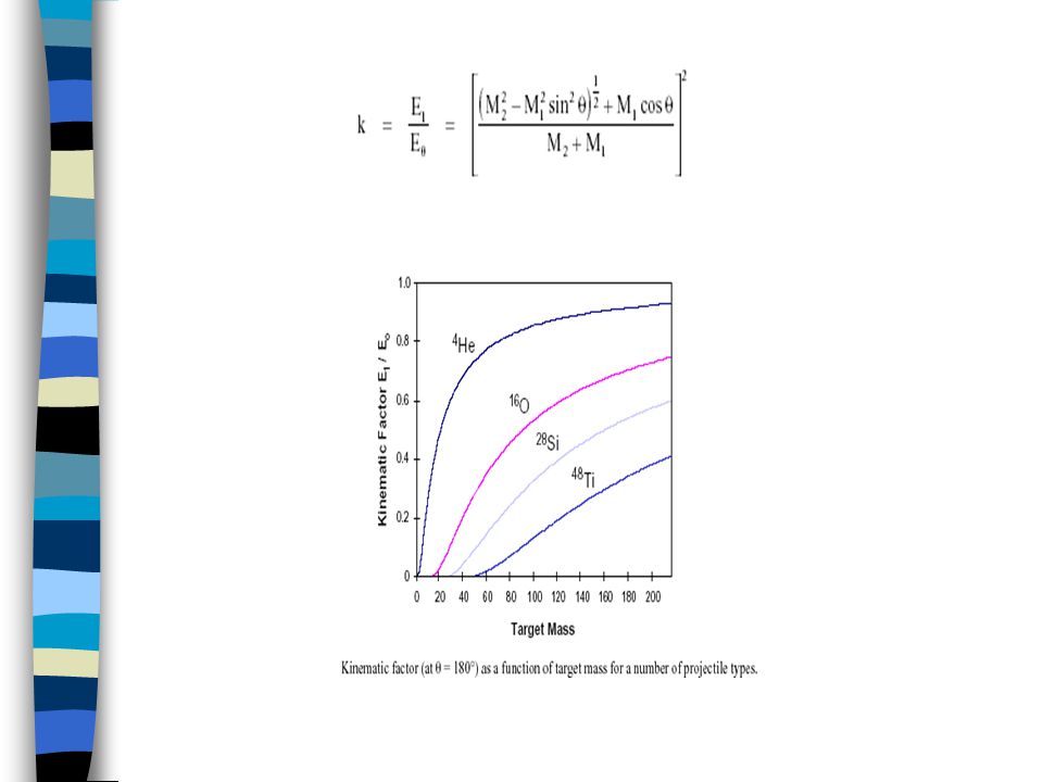
58
KINEMATIC FACTOR E can be derived from the principle of conservation of energy and momentum, and is given by (in laboratory frame of reference): The multiplication factor of E o on the right hand side of the equation is often referred to as the kinematic factor and is denoted by k. For M/m > 1, k is a slow-varying function of , having the maximum value of 1 at = 0 and the minimum value at = 180 o. For M/m = 1, the value of k is zero beyond 90 o.

63
DIFFERENTIAL SCATTERING CROSS SECTION The theoretical differential cross section for a given scattering angle is given by: The higher order terms are usually negligible for M>m and the differential cross section can be expressed in the following form, which has the unit of mb/sr (millibarn per steradian) when MeV is used as the unit for E o :
 when MeV is used as the unit for E o :")
64
A = QNt A- ukupan broj detektovanih čestica - efikasni presek rasejanja - prostorni ugao Q- ukupan broj upadnih čestica N- kocentracija atoma mete t- debljina

66
Thickness = 200A Pt Co Thickness = 1000A

71
Si Fe Ar, Xe and Au ions RBS, XRD, and CEMS analyses of solid solution and compound formation Fe x Si y Schematic view of the ion beam mixing experiments Ion energy 100-700 keV Fluence 1x10 15 -2x10 16 ions/cm 2 Liquid nitrogen room temperature Thickness 30-90nm

72
RBS spectra (a); Fe and Si concentration profiles (b) of Fe/Si bilayers irradiated with 1x10 15 - 2x10 16 Xe + ions/cm 2 at 250 keV
; Fe and Si concentration profiles (b) of Fe/Si bilayers irradiated with 1x x10 16 Xe + ions/cm 2 at 250 keV")
73
The quantitative information of the redistribution of the components across the interface Interface variance of the mixed Fe/Si bilayer 2, after RT irradiation, as a function of ion fluence (a) Ar and (b) Xe 2 / = 1.3 ± 0.2 nm 4 2 / = 4.8 ± 0.5 nm 4 k (mixing rates)
 Ar and (b) Xe 2 / = 1.3 ± 0.2 nm 4 2 / = 4.8 ± 0.5 nm 4 k (mixing rates)")
74
Interface broadening variance 2 versus ion fluence for Fe/Si bilayers irradiated with a 100 keV Ar + ions, 250 keV Xe + and 700 keV Xe 2+, and 400 keV Au + The deduced mixing rates are inserted a) linear dependece b) athermal regime c) influence of ion mass
 linear dependece b) athermal regime c) influence of ion mass")
75
RBS spectra (a); Fe and Si concentration profiles (b) of 57 Fe/Si bilayers irradiated with 0.6x10 17 - 2x10 17 N 2+ ions/cm 2 at 22 keV
; Fe and Si concentration profiles (b) of 57 Fe/Si bilayers irradiated with 0.6x x10 17 N 2+ ions/cm 2 at 22 keV")
76
500kV Jonski implanter Van de Graaff akcelerator

77
Analizatorski magnet, 500kV implanter

78
Skretni magnet VdG

79
RBS linija

80
Van de Graaff

81
Blok šema VdG generatora

82
Van de Graaff akceleratorska cev

83
Korisnici Lokacija, Zaduženje Iskorišćenost Laboratorija 040 N. Bibić Van de Graaff akcelerator 500kV Jonski implanter Istraživanja u oblasti fizike čvrstog stanja i materijala Rad u kontinuitetu od 7h, 1 uzorak 15-30 min.

Similar presentations


>")

 By Austin Avery.>")
 Fluorescent U-V Electron Monocular>")


 20823856 Özgen Buğdaycı 20824336 Elif Topçuoğlu 20823985 Yavuz Duran Hacettepe University12.04.2012.>")

, & chromoplasts.>")
