Download presentation
Presentation is loading. Please wait.

1
김해천 haecheon100@gmail.com
Memory Scaling: A System Architecture Perspective Onur Mutlu Carnegie Mellon University 김해천

2
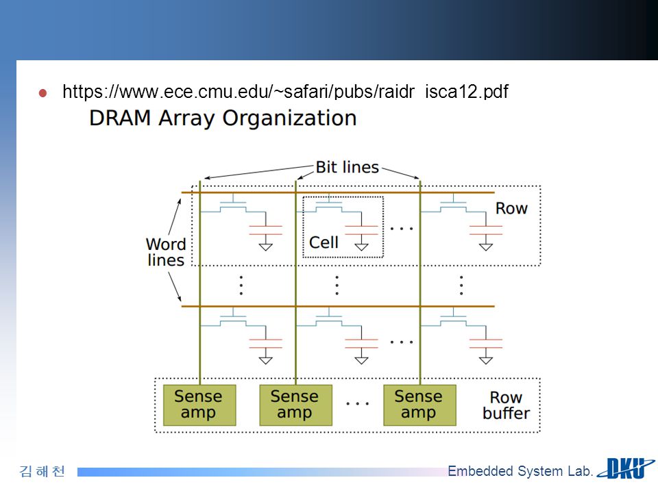
DRAM Refresh DRAM capacitor charge leak over time
The memory controller needs to refresh each row periodically to restore charge Downsides of refresh Energy consumption: Each refresh consumes energy Performance degradation: DRAM rank/bank unavailable while refreshed Refresh rate limits DRAM capacity scaling -RAIDR: Retention-Aware Intelligent DRAM Refresh -DRAM device는 가장 leakiest한 cell로 refresh 비율을 정하는데 대부분 DRAM은 상당히 오랬동안 data를 유지할 수 있어서 이러한 refresh의 많은 것이 불필요하다. -QoS/predictability impact: (Long) pause times during refresh -Refresh overhead limits DRAM scaling Refresh operations interfere with memory accesses and waste energy 디렘의 케패시터 전하는 시간이 흐름에 따라 유출 됩니다. 메모리 컨트롤러는 각각의 로우를 주기적으로 refresh하는게 필요합니다. 그런데 refresh의 좋지 않는 점이 있습니다. Refresh할 때 에너지가 소비되고, 리프레시 동안에는 해당하는 BANK를 이용할 수 없게 됩니다. 그리고 그래프에서처럼 디렘 사이즈가 커질 수록 refresh가 차지하는 performance영향이 커지게 되고, 에너지 소비도 그만큼 증가하게 되어, 디렘 공정에 제한을 만들고 있습니다. Refresh Overhead: performance Refresh Overhead: Energy
 pause times during refresh. -Refresh overhead limits DRAM scaling. Refresh operations interfere with memory accesses and waste energy. 디렘의 케패시터 전하는 시간이 흐름에 따라 유출 됩니다. 메모리 컨트롤러는 각각의 로우를 주기적으로 refresh하는게 필요합니다. 그런데 refresh의 좋지 않는 점이 있습니다. Refresh할 때 에너지가 소비되고, 리프레시 동안에는 해당하는 BANK를 이용할 수 없게 됩니다. 그리고 그래프에서처럼 디렘 사이즈가 커질 수록 refresh가 차지하는 performance영향이 커지게 되고, 에너지 소비도 그만큼 증가하게 되어, 디렘 공정에 제한을 만들고 있습니다. Refresh Overhead: performance. Refresh Overhead: Energy.")
3
Reducing Refresh Impact
Observation: High refresh rate caused by few weak DRAM Cells Problem: All cells refreshed at the same high rate Idea: RAIDR decreases refresh rate for most DRAM cells while refreshing weak cells at a higher rate Group parts of DRAM into different bins depending on their required refresh rate row’s refresh containing leaky cells > normal most rows are refreshed less frequently RAIDR: Retention-Aware Intelligent DRAM Refresh 현재의 디렘에서는 가장 약한 셀, 즉 빈번하게 refresh를 해주어야 하는 녀석을 기준으로 리프레시 비율을 정해주게 되어서 비효율적으로 리프레시가 되고 있습니다. 그런데 이렇게 자주 리프레시를 해주어야 하는 녀석들은 디렘에서 작은 양을 차지하고 있습니다. 그래서 retention aware intelligent DRAM refresh 기법을 제안했습니다. 이것의 아이디어는 Weak cell은 높은 비율로 refresh를 하고 나머지 애들은 refresh의 빈도를 줄이자는 것입니다. Profiling이라는 단계로 DRAM cell들의 refresh 해주어야 하는 빈도를 파악합니다. 그리고 binning 과정으로 파악한 빈도수를 기준으로 디렘의 부분을 나눕니다. 그리고 각 부분별로 refreshsing의 비율을 다르게 하여 진행합니다. Profiling Binning Refreshing

4
DRAM Latency and Energy
The DRAM industry: provide maximum capacity for a given cost To mitigate the high area overhead of DRAM sensing structures Connect many DRAM cells to each sense-amplifier through a wire(bitline) High parasitic capacitance Tiered-Latency DRAM: A Low Latency and Low Cost DRAM Architecture 센스 증폭기 비용을 상쇄한다 bitline이 길어지면 sense amplifier 비용이 더 커진다 -> small area가 좋다 긴 bitline의 용량은 -> high latency와 power가 필요함 트레이드 오프가 존재한다 디렘은 역사적으로 컴퓨터 시스템이 필요한 큰 용량을 제공하면서 발전해 왔습니다. 큰 area overhead를 줄이고자 디렘 cell들과 sense-amplifier를 bitline이라는 wire를 통해 연결했습니다. 이 때 bitline이 길어짐으로 인하여 기생 capacitance라는 원하지 않은 정전용량이 생긴다. 아래 그림에서도 DRAM의 Latency를 Subarray latency + I/O Latency 구별하였고 Cell들과 비트라인의 집합인 subarray latency가 주요한 녀석입니다. 디렘에서 cell의 데이터를 읽을 때 cell의 데이터를 sense amplifier가 다시 dirve해줘야 해서 더 큰 비용이 들어가게 됩니다.
 High parasitic capacitance. Tiered-Latency DRAM: A Low Latency and Low Cost DRAM Architecture. 센스 증폭기 비용을 상쇄한다. bitline이 길어지면 sense amplifier 비용이 더 커진다 -> small area가 좋다. 긴 bitline의 용량은 -> high latency와 power가 필요함. 트레이드 오프가 존재한다. 디렘은 역사적으로 컴퓨터 시스템이 필요한 큰 용량을 제공하면서 발전해 왔습니다. 큰 area overhead를 줄이고자 디렘 cell들과 sense-amplifier를 bitline이라는 wire를 통해 연결했습니다. 이 때 bitline이 길어짐으로 인하여 기생 capacitance라는 원하지 않은 정전용량이 생긴다. 아래 그림에서도 DRAM의 Latency를 Subarray latency + I/O Latency 구별하였고. Cell들과 비트라인의 집합인 subarray latency가 주요한 녀석입니다. 디렘에서 cell의 데이터를 읽을 때 cell의 데이터를 sense amplifier가 다시 dirve해줘야 해서. 더 큰 비용이 들어가게 됩니다.")
5
Reducing DRAM Latency and Energy
Challenge 1: How to efficiently migrate a row between segments? Challenge 2: How to efficiently manage the cache? 왼쪽 아래 그림을 보시면 bit line이 길어지게 된다면 high latency가 걸리게 되지만 차지하는 area아 작아지는 장점이 있고 비트라인 중간 중간에 sense amplifier를 넣어주게 된다면 sense amplifier가 serve해야 하는 비트라인이 줄어 들기 때문에 Latency는 작아지지만 차지하는 area가 커지는 단점이 있습니다. 그래서 이를 조합하여 Tiered-Latency DRAM을 제시 하였습니다. 이는 비트라인을 두 부분으로 나누는데 sense amplifier에서 가까운 영역 Near segment 먼 부분을 far segment로 구별하기 위해 가운데에 Isolation Transistor를 추가 하였습니다. 이는 일종의 스위치라고 생각하면 됩니다. 그리고 이 Near Segment 부분을 far segment의 캐시로 사용하게 됩니다. 캐쉬로 사용할 때 far segment의 row를 Near segment의 row로 옮겨야 하는 과정이 필요한데 현재의 디렘은 이 과정을 외부의 메모리 컨트롤러에서 값을 read한 다음에 다시 값을 write back해야 불필요한 과정이 필요합니다. 그래서 여기서는 그런 과정없이 Tiered-Latency DRAM 내부에서 해결합니다. 이 자세한 과정과 캐쉬에 대한 내용은 준비하지 못하였습니다.

6
RowClone: Accelerating Page Copy and Initialization
Bulk data copy and initialization Unnecessarily move data on the memory channel Degrade system performance and energy efficiency RowClone – perform copy in DRAM with low cost Uses row buffer to copy large quantity of data Source row → row buffer → destination row Accelerate Copy-on-Write and Bulk Zeroing • Forking, checkpointing, zeroing (security), VM cloning Main 메모리에서 processor cache로의 불필요한 데이터 이동 때문에 에너지와, 시간, bandwidth가 나빠진다 한 가지 예로 bulk data copy와 초기화 operation이 있는데 ( 페이지가 다른 곳으로 복사되거나, 어떠한 값으로 초기화 되는거 ) 만약에 이러한 copied data 혹은 initialized data가 즉시 프로세서에게 필요로 하지 않다면, ( 디렘에서 비교적 작은 변화들 ) DRAM안에서 이러한 operation을 수행하는 것이 에너지, bandwidth, time을 save할 수 있게 됩니다.
, VM cloning. Main 메모리에서 processor cache로의 불필요한 데이터 이동 때문에 에너지와, 시간, bandwidth가 나빠진다. 한 가지 예로 bulk data copy와 초기화 operation이 있는데 ( 페이지가 다른 곳으로 복사되거나, 어떠한 값으로 초기화 되는거 ) 만약에 이러한 copied data 혹은 initialized data가 즉시 프로세서에게 필요로 하지 않다면, ( 디렘에서 비교적 작은 변화들 ) DRAM안에서 이러한 operation을 수행하는 것이 에너지, bandwidth, time을 save할 수 있게 됩니다.")
7
RowClone: Accelerating Page Copy and Initialization
Fast Parallel Mode Pipelined Serial Mode FAST PARALLEL MODE : 둘이 같은 subarray에 있어야 함, 모든 데이터를 destination에 복사한다.

8
SALP:Reducing DRAM Bank Conflicts
Problem: Bank conflicts are costly for performance and energy serialized requests, wasted energy Goal: Reduce bank conflicts without adding more banks (low cost) Key idea: Exploit the internal subarray structure of a DRAM bank to parallelize bank conflicts to different subarrays 현재의 시스템들은 여러 멀티 스레디, 멀티 어플리케이션들이 동시에 독립적으로 메모리 리퀘스트들이 수행되는데 이런 멀티 리퀘스트들을 병럴적으로 처리하기 위해 현대의 디렘은 독립적으로 접근될 수 있는 기본 단위인 뱅크를, 멀티플 뱅크로 사용합니다. Modern DRAMs have multiple banks to serve multiple memory requests in parallel. However, when two requests go to the same bank, they have to be served serially, exacerbating the high latency of off-chip memory 그러나 같은 뱅크에 두개의 메모리 리퀘스트가 오면 동시에 처리하지 못하고 차례대로 수행하는 수 밖에 없음 뱅크를 추가하면 되지만 많은 비용이 필요하다. 이런 뱅크 conflict는 메모리 밴드위스 유틸리제이션 및 core stall, leading to lower system performance. 여기서 같은 뱅크에서 여러 리퀘스들의 레이턴시를 오버랩하는 매카니즘을 소개 row-buffer which is an array of sense-amplifiers that act as latches. Logical hierarchy of main memory DRAM bank organization
 Key idea: Exploit the internal subarray structure of a DRAM bank. to parallelize bank conflicts to different subarrays. 현재의 시스템들은 여러 멀티 스레디, 멀티 어플리케이션들이 동시에 독립적으로 메모리 리퀘스트들이 수행되는데. 이런 멀티 리퀘스트들을 병럴적으로 처리하기 위해 현대의 디렘은 독립적으로 접근될 수 있는 기본 단위인 뱅크를, 멀티플 뱅크로 사용합니다. Modern DRAMs have multiple banks to serve multiple memory requests in parallel. However, when two requests go to the. same bank, they have to be served serially, exacerbating the high latency of off-chip memory. 그러나 같은 뱅크에 두개의 메모리 리퀘스트가 오면 동시에 처리하지 못하고 차례대로 수행하는 수 밖에 없음. 뱅크를 추가하면 되지만 많은 비용이 필요하다. 이런 뱅크 conflict는 메모리 밴드위스 유틸리제이션 및 core stall, leading to lower system performance. 여기서 같은 뱅크에서 여러 리퀘스들의 레이턴시를 오버랩하는 매카니즘을 소개. row-buffer which is an array of sense-amplifiers that act as latches. Logical hierarchy of main memory. DRAM bank organization.")
9
SALP:Reducing DRAM Bank Conflicts
Subarray-Level-Parallelism 1. ACTIVATE: read the entire row into the row-buffer 2. READ/WRITE: access the column from the row-buffer 3. PRECHARGE: de-activate the row-buffer tWR : WRITE issue 후에 write recovery latency라는 추가적인 타임이 필요함. row buffer가 새로운 voltage값으로 drive될 때 안정화될 시간이 필요함. 위 아래 그림은 네 개의 requests를 service하는 모습입니다. 위에서 첫 번째 그림은 같은 뱅크에서의 모습이고 두 번째 그림은 다른 bank에서의 그림입니다. 보시는 바와 같이 다른 bank에서는 request들이 병렬처리 될 수 있지만 같은 뱅크에서는 병렬로 처리 되지 못하고 하나씩 하나씩 수행되는 모습니다. 다른 뱅크 같은 로우에 wrtie read를 할 때 Twr시간과 precharging이 생략되고 그 뒤에 write된 값을 그대로 읽은 뒤에 precharging 하면 된다. 다른 뱅크와는 독립적으로 수행되기 때문에 다른 뱅크에서 activation하고 write하는건 상관 없다. 이 논문에서는 같은 뱅크의 다른 subarray에 접근할 때의 병렬처리에 대해 설명하였는데 Subarray level parallelism 1에서는

10
Hybrid Main Memory PCM is a promising technology that can offer higher capacity than DRAM But, access latency and energy are higher than DRAM’s Endurance is lower Row buffers are the same in DRAM and PCM Row buffer hit latency same in DRAM and PCM Row buffer miss latency small in DRAM, large in PCM Row Buffer Locality Aware Caching Policies for Hybrid Memories PCM은 DRAM보다 더 작은 공정이 가능하고, cell당 multiple bit를 저장 가능하여 DRAM보다 더 큰 용량이 가능하며 Non volitile이라서 refresh가 필요없는 장점이 있지만 낮은 endurance와 access latency와 energy가 크다는 단점이 있습니다. 디렘과 PCM둘다 Row 버퍼를 캐시로 사용하는데, Row buffer hit에서는 DRAM과 PCM의 Latency가 같으나 Miss에서는 pcm의 Latency가 더 크다.

11
Hybrid Main Memory Idea: Cache in DRAM only those rows that waste
Frequently cause row buffer conflicts → because row-conflict latency is smaller in DRAM Are reused many times → to reduce cache pollution and bandwidth waste Simplified rule of thumb: Streaming accesses: Better to place in PCM Other accesses (with some reuse): Better to place in DRAM “Row Buffer Locality Aware Caching Policies for Hybrid Memories“ Simplified rule of thumb : 경험에 바탕을 둔 자주 row buffer conflicts를 야기하거나 매번 다시 사용하는 녀석들을 DRAM에 놓고 스티림한 access들을 pcm에 놓자
: Better to place in DRAM. Row Buffer Locality Aware Caching Policies for Hybrid Memories Simplified rule of thumb : 경험에 바탕을 둔. 자주 row buffer conflicts를 야기하거나 매번 다시 사용하는 녀석들을 DRAM에 놓고. 스티림한 access들을 pcm에 놓자.")
12
The End Thank you

13
참고

14
Tiered-Latency DRAM: A Low Latency and Low Cost DRAM Architecture
Inter-Segment Migration Our way: Source and destination cells share bitlines Transfer data from source to destination across shared bitlines concurrently Source Near Segment Far Segment Isolation Transistor Sense Amplifier 현재의 디램 칩에서 한 로우에서 다른 로우로 데이터를 전송할 때 ( 같은 subarray ) 데이터는 반드시 외부의 디렘 컨트롤러에게 읽혀지고 다시 칩으로 라이트 백 되어야 한다 그래서 상당히 큰 power and bandwidth 낭비, 큰 latency가 생긴다. TL-DRAM에서 데이터 전송은 전체적으로 DRAM내부에서 일어난다. ( 외부 버스의 관여 없이 ) -> 여기서 bit line이 far segment와 near segment를 연결하고 있는데 Destination
 데이터는 반드시 외부의 디렘 컨트롤러에게 읽혀지고 다시 칩으로 라이트 백 되어야 한다. 그래서 상당히 큰 power and bandwidth 낭비, 큰 latency가 생긴다. TL-DRAM에서 데이터 전송은 전체적으로 DRAM내부에서 일어난다. ( 외부 버스의 관여 없이 ) -> 여기서 bit line이 far segment와 near segment를 연결하고 있는데. Destination.")
15
Tiered-Latency DRAM: A Low Latency and Low Cost DRAM Architecture

16
SALP tRCD: row to column delay tRC: row-conflict latency
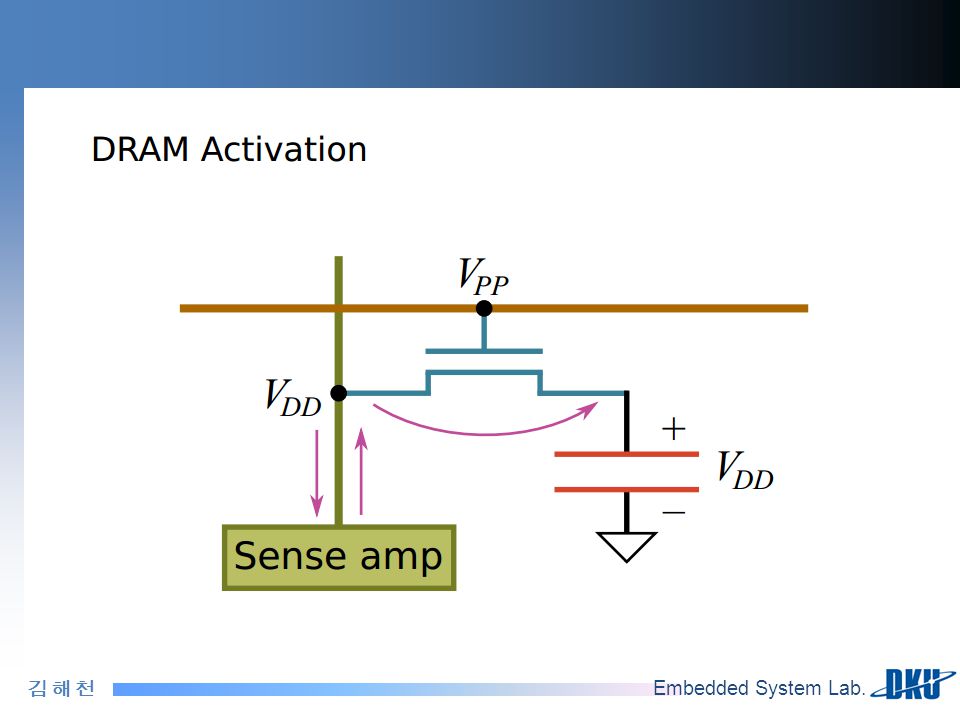
ACTIVATE Row : row-buffer로 entire row들을 읽는 과정? - 디램 low가 activated되기 전에 뱅크는 precharged state로 되어 있어야 한다. 이 상태에서 모든 비트라인들을 voltage-level of 1/2*VDD로 유지 된다. - ACTIVATE COMMAND를 ( row-address와 함께 ), 보내자마자 해당하는 wordline은 Vpp로 올려지고, connecting the row's cell to the bitlines - 그 후 cell이 충전(Q) or 비충전(0) 인지 여부에 따라 bitline voltage는 약간 VDD OR 0으로 동요된다? - 로우 버퍼는 이러한 perturbation을 감지하고, 증폭한다. - 비트라인 voltage가 transition 중에는 정의되어 있지 않는 상태다 - 비트라인 voltage가 안정화되면, cell charges는 그들의 원래의 값으로 회복된다. 이 전체시간을 tRAS라고 부른다. READ/WRITE Column - activate후에, 메모리 컨트롤러는 READ나 WRITE command를 column address와 함께 issue한다. - ACTIVATE와 그 후의 column command(READ/WRITE) 사이에 타이밍 제약은 tRCD라고 불린다 - 뱅크에게 다음의 요청이 같은 로우에 접근한다면, 이것은 column command만 있으면 된다. 이미 로우가 이미 activated되어 있기 때문에. - 그래서 새로운 row를 activate하는 것보다 더 빠르다. PRECHARGE Bank - 새로운 row를 activate하기 위해서, 메모리 컨트롤러는 첫번째로 뱅크를 precharged state로 만들어야 한다. - 이것은 두 단계로 이루어짐 - 1. 현재의 activated된 row에 해당하는 word line을 zero로 만든다. ( bitline으로 부터 cell들을 분리시키면서 ) 2. bitline들이 1/2*Vdd로 드라이븐 된다. 이러한 시간을 tRP라고 함. tRP – 먼저 activated된 subarray들이 완전히 precharged상태로 보장하기 위한 시간. tWR : WRITE issue 후에 write recovery latency라는 추가적인 타임이 필요함. row buffer가 새로운 voltage값으로 drive될 때 안정화될 시간이 필요함. 로우 버퍼가 new voltage를 drive하고 있는데, precharged 되면 전압값이 변하여 데이터의 저장이 완전해질 수 없다. tRCD: row to column delay tRC: row-conflict latency
, 보내자마자 해당하는 wordline은 Vpp로 올려지고, connecting the row s cell to the bitlines. - 그 후 cell이 충전(Q) or 비충전(0) 인지 여부에 따라 bitline voltage는 약간 VDD OR 0으로 동요된다 - 로우 버퍼는 이러한 perturbation을 감지하고, 증폭한다. - 비트라인 voltage가 transition 중에는 정의되어 있지 않는 상태다. - 비트라인 voltage가 안정화되면, cell charges는 그들의 원래의 값으로 회복된다. 이 전체시간을 tRAS라고 부른다. READ/WRITE Column - activate후에, 메모리 컨트롤러는 READ나 WRITE command를 column address와 함께 issue한다. - ACTIVATE와 그 후의 column command(READ/WRITE) 사이에 타이밍 제약은 tRCD라고 불린다. - 뱅크에게 다음의 요청이 같은 로우에 접근한다면, 이것은 column command만 있으면 된다. 이미 로우가 이미 activated되어 있기 때문에. - 그래서 새로운 row를 activate하는 것보다 더 빠르다. PRECHARGE Bank. - 새로운 row를 activate하기 위해서, 메모리 컨트롤러는 첫번째로 뱅크를 precharged state로 만들어야 한다. - 이것은 두 단계로 이루어짐 - 1. 현재의 activated된 row에 해당하는 word line을 zero로 만든다. ( bitline으로 부터 cell들을 분리시키면서 ) 2. bitline들이 1/2*Vdd로 드라이븐 된다. 이러한 시간을 tRP라고 함. tRP – 먼저 activated된 subarray들이 완전히 precharged상태로 보장하기 위한 시간. tWR : WRITE issue 후에 write recovery latency라는 추가적인 타임이 필요함. row buffer가 새로운 voltage값으로 drive될 때 안정화될 시간이 필요함. 로우 버퍼가 new voltage를 drive하고 있는데, precharged 되면 전압값이 변하여 데이터의 저장이 완전해질 수 없다. tRCD: row to column delay. tRC: row-conflict latency.")
17
SALP1 SALP2 SALP1 SALP1에서는 write recovery 시간과 activation을 overlap하지 못함
tRP(row-precharge time)은 먼저 activated된 subarray를(subarray X) precharged state로 ensure하는 시간 이미 다른 subarray가 precharged 상태라면 다른 subarray는 acrivation 시작할 수 있음. SALP1에서는 write recovery 시간과 activation을 overlap하지 못함 각 subarray의 write recovery와 activation은 자신들에 해당하는 wordline을 요청하는데, 기존의 global row-address latch는 모든 subarrays들이 공유하기 때문에 한 subarray에 해당하는 wordline만 serve할 수 있음 SALP2는 하드웨어적으로 row-address latch를 추가하여 이를 가능하게 하여 rWR과 Activation을 overlap할 수 있다.
은 먼저 activated된 subarray를(subarray X) precharged state로 ensure하는 시간. 이미 다른 subarray가 precharged 상태라면 다른 subarray는 acrivation 시작할 수 있음. SALP1에서는 write recovery 시간과 activation을 overlap하지 못함. 각 subarray의 write recovery와 activation은 자신들에 해당하는 wordline을 요청하는데, 기존의 global row-address latch는 모든 subarrays들이 공유하기 때문에 한 subarray에 해당하는 wordline만 serve할 수 있음. SALP2는 하드웨어적으로 row-address latch를 추가하여 이를 가능하게 하여 rWR과 Activation을 overlap할 수 있다.")
Similar presentations


 in DRAM Yoongu Kim, Vivek Seshadri, Donghyuk Lee, Jamie Liu, Onur Mutlu.>")


>")
>")
>")


 in DRAM Yoongu Kim, Vivek Seshadri, Donghyuk Lee, Jamie Liu, Onur Mutlu.>")


