Download presentation
Presentation is loading. Please wait.

1
DEPARTMENT OF ELECTRONICS AND COMMUNICATION
MICROPROCESSORS AND MICROCONTROLLERS By R.HARINI DEPARTMENT OF ELECTRONICS AND COMMUNICATION

2
AIM To have an in depth knowledge of the architecture and programming of 8-bit and 16-bit Microprocessors, Microcontrollers and to study how to interface various peripheral devices with them.

3
OBJECTIVE To study the architecture and Instruction set of 8085 and 8086 To develop assembly language programs in 8085 and 8086. To design and understand multiprocessor configurations To study different peripheral devices and their interfacing to 8085/8086. To study the architecture and programming of 8051 microcontroller.

4
UNIT I THE 8085 AND 8086 MICROPROCESSORS
8085 Microprocessor architecture-Addressing modes- Instruction set-Programming the 8085 UNIT II SOFTWARE ASPECTS Intel 8086 microprocessor - Architecture - Signals- Instruction Set-Addressing Modes-Assembler Directives- Assembly Language Programming-Procedures-Macros-Interrupts And Interrupt Service Routines-BIOS function calls. UNIT III MULTIPROCESSOR CONFIGURATIONS Coprocessor Configuration – Closely Coupled Configuration – Loosely Coupled Configuration –8087 Numeric Data Processor – Data Types – Architecture –8089 I/O Processor –Architecture –Communication between CPU and IOP. UNIT IV I/O INTERFACING Memory interfacing and I/O interfacing with 8085 – parallel communication interface – serial communication interface – timer-keyboard/display controller – interrupt controller – DMA controller (8237) – applications – stepper motor – temperature control. UNIT V MICROCONTROLLERS Architecture of 8051 Microcontroller – signals – I/O ports – memory – counters and timers – serial data I/O – interrupts- Interfacing -keyboard, LCD,ADC & DAC
 – applications – stepper motor – temperature control. UNIT V MICROCONTROLLERS Architecture of 8051 Microcontroller – signals – I/O ports – memory – counters and timers – serial data I/O – interrupts- Interfacing -keyboard, LCD,ADC & DAC.")
5
THE 8085 MICROPROCESSOR UNIT I 1.1 Introduction to 8085
1.2 Microprocessor architecture 1.3 Instruction set 1.4 Addressing modes 1.5 Programming the 8085.

6
PROCESSOR The first microprocessor was introduced in 1970 by Intel (named 4004). It ran at the speed of 108KHz. Four years later, Intel created the 8080 running at just over 2 Mhz. This microprocessor was used on the world's firs personal computer, named Altair. Also at this time, IBM started researching for their microprocessor, called POWER (Performance Optimization With Enhanced RISC).
.")
8
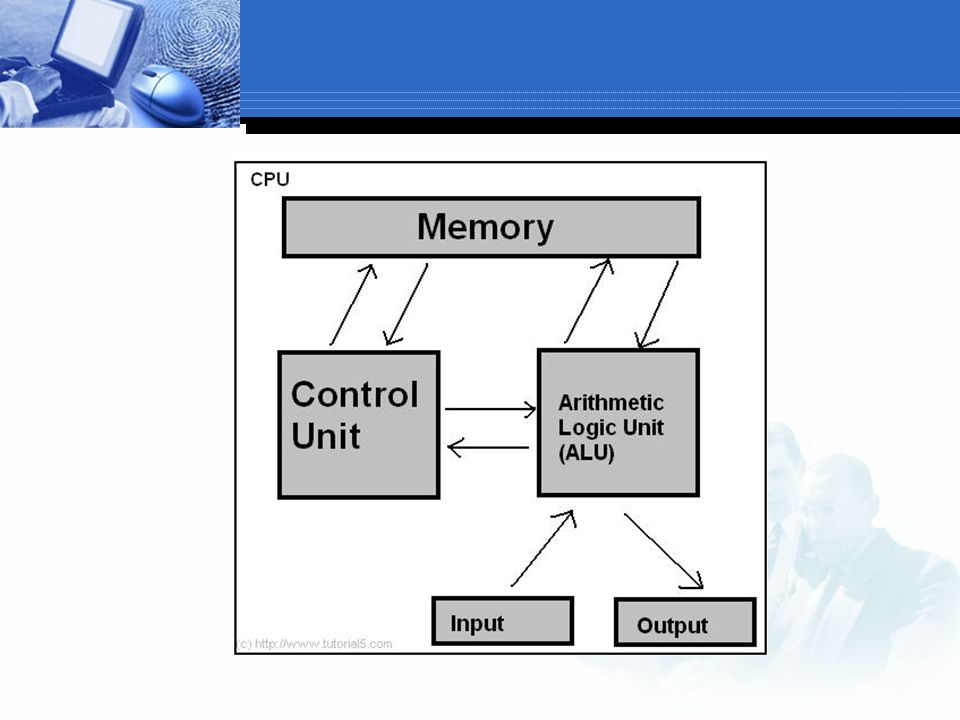
1.2 Microprocessor architecture
Control Unit Arithmetic Logic Unit Registers Accumulator Flags Program Counter (PC) Stack Pointer (SP) Instruction Register/Decoder Memory Address Register General Purpose Registers Control Generator Register Selector Microprogramming
 Stack Pointer (SP) Instruction Register/Decoder. Memory Address Register. General Purpose Registers. Control Generator. Register Selector. Microprogramming.")
9
8085 ARCHITECTURE CONTD..

10
1.3 INSTRUCTION SET BASED ON FUNCTIONS Data Transfer Instructions
Arithmetic Instructions Logical Instructions Branch Instructions Machine Control BASED ON LENGTH One-word or 1-byte instructions Two-word or 2-byte instructions Three-word or 3-byte instructions

11
8085 Instruction Set The 8085 instructions can be classified as follows: Data transfer operations Between Registers Between Memory location and a Registers Direct write to a Register/Memory Between I/O device and Accumulator Arithmetic operations (ADD, SUB, INR, DCR) Logic operations Branching operations (JMP, CALL, RET)
 Logic operations. Branching operations (JMP, CALL, RET)")
12
8085 Instruction Types

13
8085 Instruction Types

14
8085 Instruction Types

15
PIN DIAGRAM

16
1.5 ADDRESSING MODES Implied Addressing:
The addressing mode of certain instructions is implied by the instruction’s function. For example, the STC (set carry flag) instruction deals only with the carry flag, the DAA (decimal adjust accumulator) instruction deals with the accumulator. Register Addressing: Quite a large set of instructions call for register addressing. With these instructions, specify one of the registers A through E, H or L as well as the operation code. With these instructions, the accumulator is implied as a second operand. For example, the instruction CMP E may be interpreted as 'compare the contents of the E register with the contents of the accumulator. Most of the instructions that use register addressing deal with 8-bit values. However, a few of these instructions deal with 16-bit register pairs. For example, the PCHL instruction exchanges the contents of the program counter with the contents of the H and L registers. Immediate Addressing: Instructions that use immediate addressing have data assembled as a part of the instruction itself. For example, the instruction CPI 'C' may be interpreted as ‘compare the contents of the accumulator with the letter C. When assembled, this instruction has the hexadecimal value FE43. Hexadecimal 43 is the internal representation for the letter C. When this instruction is executed, the processor fetches the first instruction byte and determines that it must fetch one more byte. The processor fetches the next byte into one of its internal registers and then performs the compare operation.
 instruction deals only with the carry flag, the DAA (decimal adjust accumulator) instruction deals with the accumulator. Register Addressing: Quite a large set of instructions call for register addressing. With these instructions, specify one of the registers A through E, H or L as well as the operation code. With these instructions, the accumulator is implied as a second operand. For example, the instruction CMP E may be interpreted as compare the contents of the E register with the contents of the accumulator. Most of the instructions that use register addressing deal with 8-bit values. However, a few of these instructions deal with 16-bit register pairs. For example, the PCHL instruction exchanges the contents of the program counter with the contents of the H and L registers. Immediate Addressing: Instructions that use immediate addressing have data assembled as a part of the instruction itself. For example, the instruction CPI C may be interpreted as ‘compare the contents of the accumulator with the letter C. When assembled, this instruction has the hexadecimal value FE43. Hexadecimal 43 is the internal representation for the letter C. When this instruction is executed, the processor fetches the first instruction byte and determines that it must fetch one more byte. The processor fetches the next byte into one of its internal registers and then performs the compare operation.")
17
ADDRESSING MODES CONTD…
Direct Addressing: Jump instructions include a 16-bit address as part of the instruction. For example, the instruction JMP 1000H causes a jump to the hexadecimal address 1000 by replacing the current contents of the program counter with the new value 1000H. Instructions that include a direct address require three bytes of storage: one for the instruction code, and two for the 16-bit address Register Indirect Addressing: Register indirect instructions reference memory via a register pair. Thus, the instruction MOV M,C moves the contents of the C register into the memory address stored in the H and L register pair. The instruction LDAX B loads the accumulator with the byte of data specified by the address in the B and C register pair.

18
UNIT- II Intel 8086 microprocessor Architecture Signals
Instruction set Addressing modes Assembler directives Assembly language programming Procedures Macros Interrupts and interrupt service routines. BIOS Function Calls

19
8086 ARCHITECTURE&PIN DIAGRAM

20
8086 FEATURES 16-bit Arithmetic Logic Unit
16-bit data bus (8088 has 8-bit data bus) 20-bit address bus = 1,048,576 = 1 meg The address refers to a byte in memory. In the 8088, these bytes come in on the 8-bit data bus. In the 8086, bytes at even addresses come in on the low half of the data bus (bits 0-7) and bytes at odd addresses come in on the upper half of the data bus (bits 8-15). The 8086 can read a 16-bit word at an even address in one operation and at an odd address in two operations. The 8088 needs two operations in either case. The least significant byte of a word on an 8086 family microprocessor is at the lower address.
 20-bit address bus = 1,048,576 = 1 meg. The address refers to a byte in memory. In the 8088, these bytes come in on the 8-bit data bus. In the 8086, bytes at even addresses come in on the low half of the data bus (bits 0-7) and bytes at odd addresses come in on the upper half of the data bus (bits 8-15). The 8086 can read a 16-bit word at an even address in one operation and at an. odd address in two operations. The 8088 needs two operations in either case. The least significant byte of a word on an 8086 family microprocessor is at the. lower address.")
21
16-bit Registers

22
8086 ARCHITECTURE The 8086 has two parts, the Bus Interface Unit (BIU) and the Execution Unit (EU). The BIU fetches instructions, reads and writes data, and computes the 20-bit address. The EU decodes and executes the instructions using the 16-bit ALU. The BIU contains the following registers: IP - the Instruction Pointer CS - the Code Segment Register DS - the Data Segment Register SS - the Stack Segment Register ES - the Extra Segment Register The BIU fetches instructions using the CS and IP, written CS:IP, to contract the 20-bit address. Data is fetched using a segment register (usually the DS) and an effective address (EA) computed by the EU depending on the addressing mode.
 and an effective address (EA) computed by the EU depending on the. addressing mode.")
23
INTERNAL BLOCK

24
PROGRAM MODEL BIU registers (20 bit adder) EU registers ES
8086 Programmer’s Model ES Extra Segment BIU registers (20 bit adder) CS Code Segment SS Stack Segment DS Data Segment IP Instruction Pointer EU registers AX AH AL Accumulator BX BH BL Base Register CX CH CL Count Register DX DH DL Data Register SP Stack Pointer BP Base Pointer SI Source Index Register DI Destination Index Register FLAGS
 CS. Code Segment. SS. Stack Segment. DS. Data Segment. IP. Instruction Pointer. EU registers. AX. AH. AL. Accumulator. BX. BH. BL. Base Register. CX. CH. CL. Count Register. DX. DH. DL. Data Register. SP. Stack Pointer. BP. Base Pointer. SI. Source Index Register. DI. Destination Index Register. FLAGS.")
25
8086/88 internal registers 16 bits (2 bytes each)
AX, BX, CX and DX are two bytes wide and each byte can be accessed separately These registers are used as memory pointers. Flags will be discussed later Segment registers are used as base address for a segment in the 1 M byte of memory

26
The 8086/8088 Microprocessors: Registers
Registers are in the CPU and are referred to by specific names Data registers Hold data for an operation to be performed There are 4 data registers (AX, BX, CX, DX) Address registers Hold the address of an instruction or data element Segment registers (CS, DS, ES, SS) Pointer registers (SP, BP, IP) Index registers (SI, DI) Status register Keeps the current status of the processor On an IBM PC the status register is called the FLAGS register In total there are fourteen 16-bit registers in an 8086/8088
 Address registers. Hold the address of an instruction or data element. Segment registers (CS, DS, ES, SS) Pointer registers (SP, BP, IP) Index registers (SI, DI) Status register. Keeps the current status of the processor. On an IBM PC the status register is called the FLAGS register. In total there are fourteen 16-bit registers in an 8086/8088.")
27
Data Registers: AX, BX, CX, DX
Instructions execute faster if the data is in a register AX, BX, CX, DX are the data registers Low and High bytes of the data registers can be accessed separately AH, BH, CH, DH are the high bytes AL, BL, CL, and DL are the low bytes Data Registers are general purpose registers but they also perform special functions AX Accumulator Register Preferred register to use in arithmetic, logic and data transfer instructions because it generates the shortest Machine Language Code Must be used in multiplication and division operations Must also be used in I/O operations

28
BX CX DX Base Register Also serves as an address register
Used in array operations Used in Table Lookup operations (XLAT) CX Count register Used as a loop counter Used in shift and rotate operations DX Data register Used in multiplication and division Also used in I/O operations
 CX. Count register. Used as a loop counter. Used in shift and rotate operations. DX. Data register. Used in multiplication and division. Also used in I/O operations.")
29
Pointer and Index Registers
Contain the offset addresses of memory locations Can also be used in arithmetic and other operations SP: Stack pointer Used with SS to access the stack segment BP: Base Pointer Primarily used to access data on the stack Can be used to access data in other segments SI: Source Index register is required for some string operations When string operations are performed, the SI register points to memory locations in the data segment which is addressed by the DS register. Thus, SI is associated with the DS in string operations.

30
DI: Destination Index register
is also required for some string operations. When string operations are performed, the DI register points to memory locations in the data segment which is addressed by the ES register. Thus, DI is associated with the ES in string operations. The SI and the DI registers may also be used to access data stored in arrays

31
Segment Registers - CS, DS, SS and ES
Are Address registers Store the memory addresses of instructions and data Memory Organization Each byte in memory has a 20 bit address starting with 0 to or 1 meg of addressable memory Addresses are expressed as 5 hex digits from FFFFF Problem: But 20 bit addresses are TOO BIG to fit in 16 bit registers! Solution: Memory Segment Block of 64K (65,536) consecutive memory bytes A segment number is a 16 bit number Segment numbers range from 0000 to FFFF Within a segment, a particular memory location is specified with an offset An offset also ranges from 0000 to FFFF
 consecutive memory bytes. A segment number is a 16 bit number. Segment numbers range from 0000 to FFFF. Within a segment, a particular memory location is specified with an offset. An offset also ranges from 0000 to FFFF.")
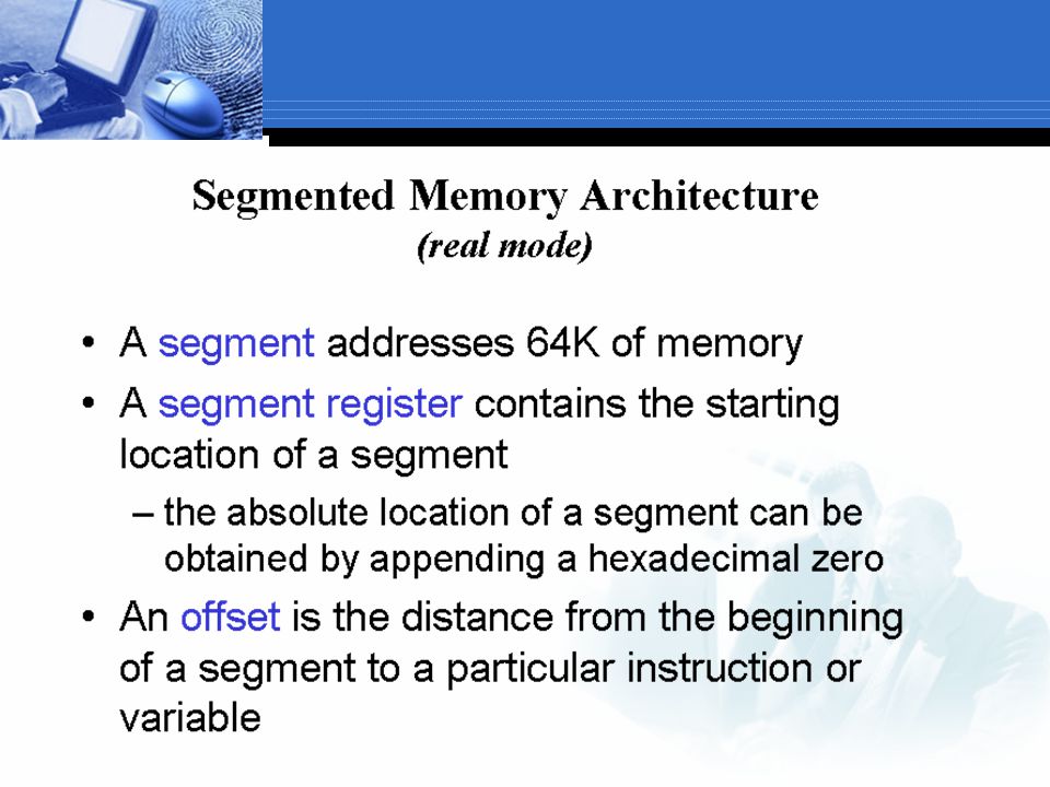
33
Segmented Memory Segmented memory addressing: absolute (linear) address is a combination of a 16-bit segment value added to a 16-bit offset one segment linear addresses

34
Memory Address Generation
Intel Memory Address Generation The BIU has a dedicated adder for determining physical memory addresses Offset Value (16 bits) Segment Register (16 bits) Adder Physical Address (20 Bits)
 Segment Register (16 bits) Adder. Physical Address (20 Bits)")
35
Example Address Calculation
Intel Example Address Calculation If the data segment starts at location 1000h and a data reference contains the address 29h where is the actual data? 2 9 Offset: Segment: Address:

36
SEGMENT:OFFSET ADDRESS
Logical Address is specified as segment:offset Physical address is obtained by shifting the segment address 4 bits to the left and adding the offset address Thus the physical address of the logical address A4FB:4872 is A4FB0 + 4872 A9822

37
EXAMPLE

38
The physical address is also called the absolute address.
THE CODE SEGMENT 0H Memory + CS: IP 0400H 0056H 4000H 4056H 0400 0056 04056H The offset is the distance in bytes from the start of the segment. The offset is given by the IP for the Code Segment. Instructions are always fetched with using the CS register. The physical address is also called the absolute address. CS:IP = 400:56 Logical Address Segment Register Offset Physical or Absolute Address 0FFFFFH

39
0H 0FFFFFH Memory Segment Register Offset Physical Address + DS: EA
THE DATA SEGMENT Memory Segment Register Offset Physical Address + DS: EA 05C0 0050 05C00H 05C50H DS:EA 0H 0FFFFFH Data is usually fetched with respect to the DS register. The effective address (EA) is the offset. The EA depends on the addressing mode.
 is the offset. The EA depends on the addressing mode.")
40
The stack grows toward decreasing memory locations.
THE STACK SEGMENT Memory + SS: SP 0A00 0100 0A000H 0A100H The stack is always referenced with respect to the stack segment register. The stack grows toward decreasing memory locations. The SP points to the last or top item on the stack. PUSH - pre-decrement the SP POP - post-increment the SP The offset is given by the SP register. SS:SP 0H 0FFFFFH Segment Register Offset Physical Address

41
Flags Carry flag Overflow Parity flag Direction Interrupt enable Auxiliary flag Trap Zero Sign 6 are status flags 3 are control flag

42
Flag Register Conditional flags: They are set according to some results of arithmetic operation. You do not need to alter the value yourself. Control flags: Used to control some operations of the MPU. These flags are to be set by you in order to achieve some specific purposes. Flag O D I T S Z A P C Bit no. 15 14 13 12 11 10 9 8 7 6 5 4 3 2 1 CF (carry) Contains carry from leftmost bit following arithmetic, also contains last bit from a shift or rotate operation.
 Contains carry from leftmost bit following arithmetic, also contains last bit from a shift or rotate operation.")
43
Flag Register OF (overflow) Indicates overflow of the leftmost bit during arithmetic. DF (direction) Indicates left or right for moving or comparing string data. IF (interrupt) Indicates whether external interrupts are being processed or ignored. TF (trap) Permits operation of the processor in single step mode.
 Indicates left or right for moving or comparing string data. IF (interrupt) Indicates whether external interrupts are being processed or ignored. TF (trap) Permits operation of the processor in single step mode.")
44
SF (sign) Contains the resulting sign of an arithmetic operation (1=negative)
ZF (zero) Indicates when the result of arithmetic or a comparison is zero. (1=yes) AF (auxiliary carry) Contains carry out of bit 3 into bit 4 for specialized arithmetic. PF (parity) Indicates the number of 1 bits that result from an operation.
 Indicates when the result of arithmetic or a comparison is zero. (1=yes) AF (auxiliary carry) Contains carry out of bit 3 into bit 4 for specialized arithmetic. PF (parity) Indicates the number of 1 bits that result from an operation.")
45
Macros avoid repetitious SAS code
create generalizable and flexible SAS code pass information from one part of a SAS job to another conditionally execute data steps and PROCs dynamically create code at execution time

46
proc contents data=&dsn; proc print data=&dsn(obs=10);
Example Simple macro variable %let dsn=LAB; title "DATA SET &dsn"; proc contents data=&dsn; run; proc print data=&dsn(obs=10);
;")
47
Procedures Initial call to run an external program
Run a LCA model to simulate data Estimate a model of simulated data Collect necessary output Check if output read is indeed output wanted Collect output in a single data matrix

48
Instruction Set Mov destination, source
add, inc, dec and sub instructions Input/Output String Instructions Machine Control Flag Manipulation.

49
Addressing Modes Immediate addressing. Register addressing.
Direct addressing. Indirect addressing Implied addressing. Indexed addressing Relative addressing

50
Interrupts &Interrupt Service Routine
An interrupt signals the processor to suspend its current activity (i.e. running your program) and to pass control to an interrupt service program (i.e. part of the operating system). A software interrupt is one generated by a program (as opposed to one generated by hardware). The 8086 int instruction generates a software interrupt. It uses a single operand which is a number indicating which MSDOS subprogram is to be invoked. This subprogram handles a variety of I/O operations by calling appropriate subprograms.
 and to pass control to an interrupt service program (i.e. part of the operating system). A software interrupt is one generated by a program (as opposed to. one generated by hardware). The 8086 int instruction generates a software interrupt. It uses a single operand which is a number indicating which MSDOS. subprogram is to be invoked. This subprogram handles a variety of I/O operations by calling. appropriate subprograms.")
51
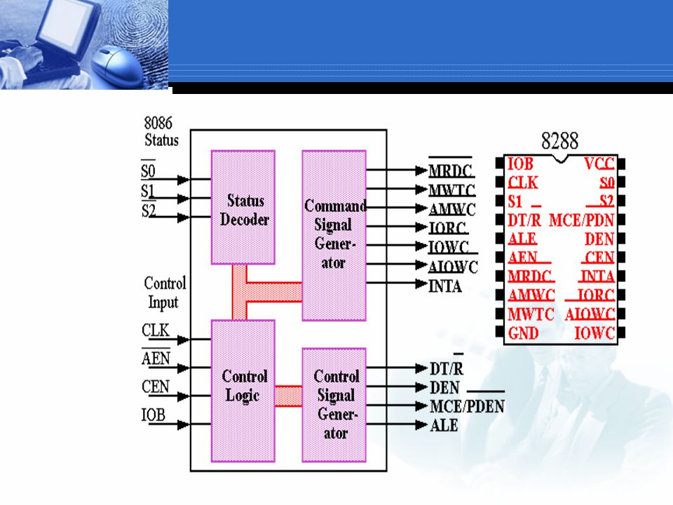
MAXIMUM MODE Maximum mode
Maximum mode is designed to be used with a coprocessor exists in the system. All the control signals (except RD) are not generated by the microprocessor. But we still need those control signals. Solution: 8288.
 are not generated by the microprocessor. But we still need those control signals. Solution:")
52
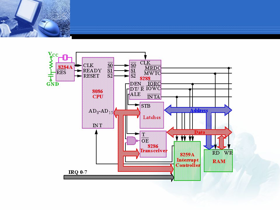
8086 maximum & minimum modes
The mode is controlled by MN/MX. Maximum mode is obtained by connecting MN/MX to low and minimum mode is by connecting it to high. Having two different modes (minimum and maximum) is used only 8088/8086. Each mode enables a different control structure. Minimum mode operation and control signals are very similar to those of 8085. So bit peripherals can be used with 8086 without special considerations. Easy and least expensive way to build single processor systems
 is used only 8088/8086. Each mode enables a different control structure. Minimum mode operation and control signals are very similar to those of So bit peripherals can be used with 8086 without special considerations. Easy and least expensive way to build single processor systems.")
54
0 1 0 Write I/O port IOWC, AIOWC 0 1 1 Halt none
S2 S1 S operation signal Interrupt Acknowledge INTA Read I/O port IORC Write I/O port IOWC, AIOWC Halt none Instruction Fetch MRDC Read Memory MRDC Write Memory MWTC, AMWC Passive none

56
UNIT III Coprocessor Configuration Closely Coupled Configuration
Loosely Coupled Configuration 8087 Numeric Data Processor-architecture Data types 8089 I/O Processor-Architecture Communication between CPU and IOP

57
PIN DIAGRAM OF 8087

58
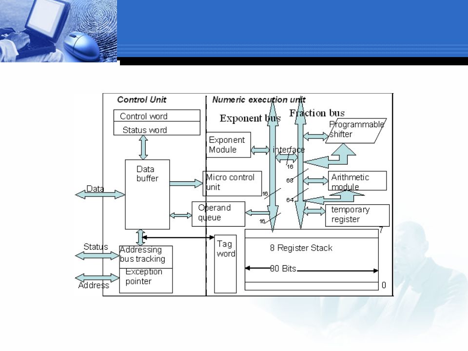
Architecture of 8087 Two Units Control Unit Execution Unit

60
Control Unit Status Register
Control unit: To synchronize the operation of the coprocessor and the processor. This unit has a Control word and Status word and Data Buffer If instruction is an ESCape (coprocessor) instruction, the coprocessor executes it, if not the microprocessor executes. Status register reflects the over all operation of the coprocessor. Status Register
 instruction, the coprocessor executes it, if not. the microprocessor executes. Status register reflects the over all operation of the coprocessor. Status Register.")
61
Status Register C3-C0 Condition code bits TOP Top-of-stack (ST)
ES Error summary PE Precision error UE Under flow error OE Overflow error ZE Zero error DE Denormalized error IE Invalid error B Busy bit B-Busy bit indicates that coprocessor is busy executing a task. Busy can be tested by examining the status or by using the FWAIT instruction. C3-C0 Condition code bits indicates conditions about the coprocessor. TOP- Top of the stack (ST) bit indicates the current register address as the top of the stack. ES-Error summary bit is set if any unmasked error bit (PE, UE, OE, ZE, DE, or IE) is set. In the 8087 the error summary is also caused a coprocessor interrupt. PE- Precision error indicates that the result or operand executes selected precision. UE-Under flow error indicates the result is too large to be represent with the current precision selected by the control word. OE-Over flow error indicates a result that is too large to be represented. If this error is masked, the coprocessor generates infinity for an overflow error. ZE-A Zero error indicates the divisor was zero while the dividend is a non-infinity or non-zero number. DE-Denormalized error indicates at least one of the operand is denormalized. IE-Invalid error indicates a stack overflow or underflow, indeterminate from (0/0,0,-0, etc) or the use of a NAN as an operand. This flag indicates error such as those produced by taking the square root of a negative number.
 bit indicates the current register address as the top of the stack. ES-Error summary bit is set if any unmasked error bit (PE, UE, OE, ZE, DE, or IE) is set. In the 8087 the error summary is also caused a coprocessor interrupt. PE- Precision error indicates that the result or operand executes selected precision. UE-Under flow error indicates the result is too large to be represent with the current precision selected by the control word. OE-Over flow error indicates a result that is too large to be represented. If this error is masked, the coprocessor generates infinity for an overflow error. ZE-A Zero error indicates the divisor was zero while the dividend is a non-infinity or non-zero number. DE-Denormalized error indicates at least one of the operand is denormalized. IE-Invalid error indicates a stack overflow or underflow, indeterminate from (0/0,0,-0, etc) or the use of a NAN as an operand. This flag indicates error such as those produced. by taking the square root of a negative number.")
62
CONTROL REGISTER Control register selects precision, rounding control, infinity control. It also masks an unmasks the exception bits that correspond to the rightmost Six bits of status register. Instruction FLDCW is used to load the value into the control register. IC Infinity control RC Rounding control PC Precision control PM Precision control UM Underflow mask OM Overflow mask ZM Division by zero mask DM Denormalized operand mask IM Invalid operand mask

63
RC –Rounding control determines the type of rounding. ROUNDING CONTROL
IC –Infinity control selects either affine or projective infinity. Affine allows positive and negative infinity, while projective assumes infinity is unsigned. INFINITY CONTROL 0 = Projective 1 = Affine RC –Rounding control determines the type of rounding. ROUNDING CONTROL 00=Round to nearest or even 01=Round down towards minus infinity 10=Round up towards plus infinity 11=Chop or truncate towards zero PC- Precision control sets the precision of he result as define in table PRECISION CONTROL 00=Single precision (short) 01=Reserved 10=Double precision (long) 11=Extended precision (temporary) Exception Masks – It Determines whether the error indicated by the exception affects the error bit in the status register. If a logic1 is placed in one of the exception control bits, corresponding status register bit is masked off.
 01=Reserved. 10=Double precision (long) 11=Extended precision (temporary) Exception Masks – It Determines whether the error indicated by the exception affects. the error bit in the status register. If a logic1 is placed in one of the exception control bits, corresponding status register bit is masked off.")
64
Numeric Execution Unit
This performs all operations that access and manipulate the numeric data in the coprocessor’s registers. Numeric registers in NUE are 80 bits wide. NUE is able to perform arithmetic, logical and transcendental operations as well as supply a small number of mathematical constants from its on-chip ROM. Numeric data is routed into two parts ways a 64 bit mantissa bus and a 16 bit sign/exponent bus.

65
Data Types Internally, all data operands are converted to the 80-bit temporary real format. We have 3 types. Integer data type Packed BCD data type Real data type Example Converting a decimal number into a Floating-point number. 1) Converting the decimal number into binary form. 2) Normalize the binary number 3) Calculate the biased exponent. 4) Store the number in the floating-point format. Step Result 1) 2) = * 26 3) = 4 ) Sign = 0 Exponent = Significand = In step 3 the biased exponent is the exponent a 26 or 110,plus a bias of (7FH) single precision no use 7F and double precision no use 3FFFH. IN step 4 the information found in prior step is combined to form the floating point no.
 Converting the decimal number into binary form. 2) Normalize the binary number. 3) Calculate the biased exponent. 4) Store the number in the floating-point format. Step Result. 1) ) = * 26. 3) = ) Sign = 0. Exponent = Significand = In step 3 the biased exponent is the exponent a 26 or 110,plus a bias of (7FH) single precision no use 7F and double precision no use 3FFFH. IN step 4 the information found in prior step is combined to form the floating point no.")
66
UNIT V Architecture of 8051 Signals Operational features
Memory and I/O addressing Interrupts Instruction set Applications.

67
Microcontroller : A single chip A smaller computer
On-chip RAM, ROM, I/O ports... Example:Motorola’s 6811, Intel’s 8051, Zilog’s Z8 and PIC 16X CPU RAM ROM A single chip Serial COM Port I/O Port Timer Microcontroller

68
Microprocessor vs. Microcontroller
CPU is stand-alone, RAM, ROM, I/O, timer are separate designer can decide on the amount of ROM, RAM and I/O ports. expansive versatility general-purpose Microcontroller CPU, RAM, ROM, I/O and timer are all on a single chip fix amount of on-chip ROM, RAM, I/O ports for applications in which cost, power and space are critical single-purpose versatility 多用途的: any number of applications for PC

69
Block Diagram External interrupts On-chip ROM for program code
Timer/Counter Interrupt Control On-chip RAM Timer 1 Counter Inputs Timer 0 CPU Serial Port Bus Control 4 I/O Ports OSC P0 P1 P2 P3 TxD RxD Address/Data

70
Pin Description of the 8051 8051 (8031) 1 2 3 4 5 6 7 8 9 10 11 12
13 14 15 16 17 18 19 20 40 39 38 37 36 35 34 33 32 31 30 29 28 27 26 25 24 23 22 21 P1.0 P1.1 P1.2 P1.3 P1.4 P1.5 P1.6 P1.7 RST (RXD)P3.0 (TXD)P3.1 (T0)P3.4 (T1)P3.5 XTAL2 XTAL1 GND (INT0)P3.2 (INT1)P3.3 (RD)P3.7 (WR)P3.6 Vcc P0.0(AD0) P0.1(AD1) P0.2(AD2) P0.3(AD3) P0.4(AD4) P0.5(AD5) P0.6(AD6) P0.7(AD7) EA/VPP ALE/PROG PSEN P2.7(A15) P2.6(A14) P2.5(A13) P2.4(A12) P2.3(A11) P2.2(A10) P2.1(A9) P2.0(A8) 8051 (8031)
P3.0. (TXD)P3.1. (T0)P3.4. (T1)P3.5. XTAL2. XTAL1. GND. (INT0)P3.2. (INT1)P3.3. (RD)P3.7. (WR)P3.6. Vcc. P0.0(AD0) P0.1(AD1) P0.2(AD2) P0.3(AD3) P0.4(AD4) P0.5(AD5) P0.6(AD6) P0.7(AD7) EA/VPP. ALE/PROG. PSEN. P2.7(A15) P2.6(A14) P2.5(A13) P2.4(A12) P2.3(A11) P2.2(A10) P2.1(A9) P2.0(A8) (8031) ")
71
Figure (b). Power-On RESET Circuit
Vcc + 10 uF 31 EA/VPP X1 30 pF 19 MHz 8.2 K X2 18 30 pF RST 9

72
Port 0 with Pull-Up Resistors
DS5000 8751 8951 Vcc 10 K Port 0

73
Some 8-bitt Registers of the 8051
A B R0 R1 R3 R4 R2 R5 R7 R6 DPH DPL PC DPTR Some bit Register Some 8-bitt Registers of the 8051

74
Stack in the 8051 The register used to access the stack is called SP (stack pointer) register. The stack pointer in the 8051 is only 8 bits wide, which means that it can take value 00 to FFH. When 8051 powered up, the SP register contains value 07. 7FH 30H 2FH 20H 1FH 17H 10H 0FH 07H 08H 18H 00H Register Bank 0 (Stack) Register Bank 1 Register Bank 2 Register Bank 3 Bit-Addressable RAM Scratch pad RAM
 Register Bank 1. Register Bank 2. Register Bank 3. Bit-Addressable RAM. Scratch pad RAM.")
75
Timer : Timer: :

76
Interrupt :

77
Numerical Bases Used in Programming
Hexadecimal Binary BCD

78
Hexadecimal Basis Hexadecimal Digits: 1 2 3 4 5 6 7 8 9 A B C D E F

79
Decimal, Binary, BCD, & Hexadecimal Numbers
(43)10= ( )BCD= ( )2 = ( B )16
10= ( )BCD= ( )2 = ( 2 B )16.")
80
MOV Rn, A ;n=0,..,7 ADD A, Rn MOV DPL, R6 MOV DPTR, A MOV Rm, Rn
Register Addressing Mode MOV Rn, A ;n=0,..,7 ADD A, Rn MOV DPL, R6 MOV DPTR, A MOV Rm, Rn

81
Direct Addressing Mode
Although the entire of 128 bytes of RAM can be accessed using direct addressing mode, it is most often used to access RAM loc. 30 – 7FH. MOV R0, 40H MOV 56H, A MOV A, 4 ; ≡ MOV A, R4 MOV 6, 2 ; copy R2 to R6 ; MOV R6,R2 is invalid !

82
Immediate Addressing Mode
MOV A,#65H MOV R6,#65H MOV DPTR,#2343H MOV P1,#65H

83
SETB bit ; bit=1 CLR bit ; bit=0 SETB C ; CY=1
SETB P0.0 ;bit 0 from port 0 =1 SETB P3.7 ;bit 7 from port 3 =1 SETB ACC.2 ;bit 2 from ACCUMULATOR =1 SETB 05 ;set high D5 of RAM loc. 20h Note: CLR instruction is as same as SETB i.e.: CLR C ;CY=0 But following instruction is only for CLR: CLR A ;A=0

84
DEC byte ;byte=byte-1 INC byte ;byte=byte+1 INC R7 DEC A
DEC 40H ; [40]=[40]-1

85
LOOP and JUMP Instructions
Conditional Jumps : JZ Jump if A=0 JNZ Jump if A/=0 DJNZ Decrement and jump if A/=0 CJNE A,byte Jump if A/=byte CJNE reg,#data Jump if byte/=#data JC Jump if CY=1 JNC Jump if CY=0 JB Jump if bit=1 JNB Jump if bit=0 JBC Jump if bit=1 and clear bit

86
Call instruction SETB P0.0 . CALL UP CLR P0.0 RET UP:

87
UNIT IV Memory Interfacing and I/O interfacing
Parallel communication interface Serial communication interface Timer Keyboard /display controller Interrupt controller DMA controller Programming and applications

88
Accessing I/O Devices I/O address mapping Memory-mapped I/O
Reading and writing are similar to memory read/write Uses same memory read and write signals Most processors use this I/O mapping Isolated I/O Separate I/O address space Separate I/O read and write signals are needed Pentium supports isolated I/O 64 KB address space Can be any combination of 8-, 16- and 32-bit I/O ports Also supports memory-mapped I/O

89
Accessing I/O Devices (cont’d)
Accessing I/O ports in Pentium Register I/O instructions in accumulator, port8 ; direct format Useful to access first 256 ports in accumulator,DX ; indirect format DX gives the port address Block I/O instructions ins and outs Both take no operands---as in string instructions ins: port address in DX, memory address in ES:(E)DI outs: port address in DX, memory address in ES:(E)SI We can use rep prefix for block transfer of data
DI. outs: port address in DX, memory address in ES:(E)SI. We can use rep prefix for block transfer of data.")
90
An Example I/O Device Keyboard Keyboard controller scans and reports
Key depressions and releases Supplies key identity as a scan code Scan code is like a sequence number of the key Key’s scan code depends on its position on the keyboard No relation to the ASCII value of the key Interfaced through an 8-bit parallel I/O port Originally supported by 8255 programmable peripheral interface chip (PPI)
")
91
An Example I/O Device (cont’d)
8255 PPI has three 8-bit registers Port A (PA) Port B (PB) Port C (PC) These ports are mapped as follows 8255 register Port address PA (input port) 60H PB (output port) 61H PC (input port) 62H Command register 63H
 Port B (PB) Port C (PC) These ports are mapped as follows register Port address. PA (input port) 60H. PB (output port) 61H. PC (input port) 62H. Command register 63H.")
92
An Example I/O Device (cont’d)
Mapping of 8255 I/O ports

93
An Example I/O Device (cont’d)
Mapping I/O ports is similar to mapping memory Partial mapping Full mapping See our discussion in Chapter 16 Keyboard scan code and status can be read from port 60H 7-bit scan code is available from PA0 – PA6 Key status is available from PA7 PA7 = 0 – key depressed PA0 = 1 – key released

94
I/O Data Transfer Data transfer involves two phases
A data transfer phase It can be done either by Programmed I/O DMA An end-notification phase Interrupt Three basic techniques Interrupt-driven I/O (discussed in Chapter 20)
")
95
I/O Data Transfer (cont’d)
Programmed I/O Done by busy-waiting This process is called polling Example Reading a key from the keyboard involves Waiting for PA7 bit to go low Indicates that a key is pressed Reading the key scan code Translating it to the ASCII value Waiting until the key is released Program 19.1 uses this process to read input from the keyboard

96
I/O Data Transfer (cont’d)
Direct memory access (DMA) Problems with programmed I/O Processor wastes time polling In our example Waiting for a key to be pressed, Waiting for it to be released May not satisfy timing constraints associated with some devices Disk read or write DMA Frees the processor of the data transfer responsibility
 Problems with programmed I/O. Processor wastes time polling. In our example. Waiting for a key to be pressed, Waiting for it to be released. May not satisfy timing constraints associated with some devices. Disk read or write. DMA. Frees the processor of the data transfer responsibility.")
97
I/O Data Transfer (cont’d)
")
98
I/O Data Transfer (cont’d)
DMA is implemented using a DMA controller DMA controller Acts as slave to processor Receives instructions from processor Example: Reading from an I/O device Processor gives details to the DMA controller I/O device number Main memory buffer address Number of bytes to transfer Direction of transfer (memory I/O device, or vice versa)
")
99
I/O Data Transfer (cont’d)
Steps in a DMA operation Processor initiates the DMA controller Gives device number, memory buffer pointer, … Called channel initialization Once initialized, it is ready for data transfer When ready, I/O device informs the DMA controller DMA controller starts the data transfer process Obtains bus by going through bus arbitration Places memory address and appropriate control signals Completes transfer and releases the bus Updates memory address and count value If more to read, loops back to repeat the process Notify the processor when done Typically uses an interrupt

100
I/O Data Transfer (cont’d)
DMA controller details

101
I/O Data Transfer (cont’d)
DMA transfer timing

102
I/O Data Transfer (cont’d)
8237 DMA controller

103
I/O Data Transfer (cont’d)
8237 supports four DMA channels It has the following internal registers Current address register One 16-bit register for each channel Holds address for the current DMA transfer Current word register Keeps the byte count Generates terminal count (TC) signal when the count goes from zero to FFFFH Command register Used to program 8257 (type of priority, …)
 signal when the count goes from zero to FFFFH. Command register. Used to program 8257 (type of priority, …)")
104
I/O Data Transfer (cont’d)
Mode register Each channel can be programmed to Read or write Autoincrement or autodecrement the address Autoinitialize the channel Request register For software-initiated DMA Mask register Used to disable a specific channel Status register Temporary register Used for memory-to-memory transfers

105
Interrupt to Processor
What is a Timer? A device that uses highspeed clock input to provide a series of time or count-related events Counter Register System Clock 0x1206 Reload on Zero ÷ 000000 Clock Divider Countdown Register Interrupt to Processor I/O Control

106
Inside the Timer High Byte Low Byte Counter Register GO Register
at offsets 0x04, 0x00 (write only) GO Register offset 0x08, immediately moves Counter Reg value into Current Counter Current Counter (not directly readable by software) Latch Register offset 0x0C, write a ``1'' to immediately write Current Counter value to readable Latch Reg Latched Counter at offsets 0x04, 0x00 (read only)
 GO Register. offset 0x08, immediately moves. Counter Reg value into Current Counter. Current Counter. (not directly readable by software) Latch Register. offset 0x0C, write a ``1 to immediately write. Current Counter value to readable Latch Reg. Latched Counter. at offsets 0x04, 0x00 (read only)")
107
Setting the Timer's Counter Registers
Counter is usually programmed to reach zero X times per second To program the timer to reach zero 100 times per second Example: For a 2 MHz-based timer, 2MHz / 100 = 20,000 #define TIMER1 0x int time; time = / 100; timer = (timer_p) TIMER1; timer>countLow = (unsigned char) (time & 0xff); timer>countHigh = (unsigned char) ((time > 8) & 0xff); timer>go = (unsigned char) 0x1;
 TIMER1; timer>countLow = (unsigned char) (time & 0xff); timer>countHigh = (unsigned char) ((time > 8) & 0xff); timer>go = (unsigned char) 0x1;")
108
Interrupt vs. Polled I/O
Polled I/O requires the CPU to ask a device (e.g. toggle switches) if the device requires servicing For example, if the toggle switches have changed position Software plans for polling the devices and is written to know when a device will be serviced Interrupt I/O allows the device to interrupt the processor, announcing that the device requires attention This allows the CPU to ignore devices unless they request servicing (via interrupts) Software cannot plan for an interrupt because interrupts can happen at any time therefore, software has no idea when an interrupt will occur This makes it more difficult to write code Processors can be programmed to ignore interrupts We call this masking of interrupts Different types of interrupts can be masked (IRQ vs. FIQ)
 if the device requires servicing. For example, if the toggle switches have changed position. Software plans for polling the devices and is written to know when a device will be serviced. Interrupt I/O allows the device to interrupt the processor, announcing that the device requires attention. This allows the CPU to ignore devices unless they request servicing (via interrupts) Software cannot plan for an interrupt because interrupts can happen at any time therefore, software has no idea when an interrupt will occur. This makes it more difficult to write code. Processors can be programmed to ignore interrupts. We call this masking of interrupts. Different types of interrupts can be masked (IRQ vs. FIQ)")
109
IRQ and FIQ Program Status Register N
To disable interrupts, set the corresponding “F” or “I” bit to 1 On interrupt, processor switches to FIQ32_mode registers or IRQ32_mode registers On any interrupt (or) Switch register banks Copy PC and CPSR to R14 and SPSR Change new CPSR mode bits SWI Trap N … Z C V I F M4 M3 M2 M1 M0
 Switch register banks. Copy PC and CPSR to R14 and SPSR. Change new CPSR mode bits. SWI Trap. N … Z. C. V. I. F. M4. M3. M2. M1. M0.")
110
INTERFACING Static RAM interfacing. Procedure Configuration.
Dynamic RAM interfacing.

111
I/O Port Interfacing Steps in Interfacing Methods of interfacing
a) I/O Mapped b) Memory Mapped.
 I/O Mapped. b) Memory Mapped.")
112
PIO 8255 Programmable input output Port. Architecture Signals
Modes Of Operation BSR Mode I/O Modes Mode 0(Basic I/O Mode) Mode 1 (Strobed I/O Mode) Mode 2 (Strobed Bidirectional Mode)
 Mode 1 (Strobed I/O Mode) Mode 2 (Strobed Bidirectional Mode)")
113
Controller 8259 Programmable Interrupt Controller.
Architecture and Signal Descriptions Interrupt Sequence . Command word Initialization Command word (ICWs). Operation Command words. Modes of operation: 1.Nested mode. 2.Fully Nested Mode. 3.Poll mode Automatic EOI Mode.
. Operation Command words. Modes of operation: 1.Nested mode. 2.Fully Nested Mode. 3.Poll mode. Automatic EOI Mode.")
114
Display Controller 8279 Output Mode 1)Display Scan 2) Display Entry
Command words.

115
8251 USART Methods of Data communication a) Simplex b) Duplex
c) Half Duplex Architecture Control Word Mode Instruction control word Command instruction control word
 Half Duplex. Architecture. Control Word. Mode Instruction control word. Command instruction control word.")
116
TEXT BOOKS Ramesh S.Gaonkar, “Microprocessor - Architecture, Programming and Applications with the 8085”, Penram International publishing private limited, fifth edition. (UNIT-1: – Chapters 3,5,6 and programming examples from chapters 7-10) A.K. Ray & K.M.Bhurchandi, “Advanced Microprocessors and peripherals- Architectures, Programming and Interfacing”, TMH, 2002 reprint. (UNITS 2 to 5: – Chapters 1-6, , 8, 16)
 A.K. Ray & K.M.Bhurchandi, Advanced Microprocessors and peripherals- Architectures, Programming and Interfacing , TMH, 2002 reprint. (UNITS 2 to 5: – Chapters 1-6, , 8, 16)")
117
REFERENCES Douglas V.Hall, “Microprocessors and Interfacing: Programming and Hardware”, TMH, Third edition Yu-cheng Liu, Glenn A.Gibson, “Microcomputer systems: The 8086 / 8088 Family architecture, Programming and Design”, PHI 2003 Mohamed Ali Mazidi, Janice Gillispie Mazidi, “The 8051 microcontroller and embedded systems”, Pearson education, 2004.

Similar presentations


 By Dr. Syed Noman.>")

>")

 1 Prepared By: Associate Prof. Dr Masri Ayob.>")
 Microprocessor.>")


