Download presentation
Presentation is loading. Please wait.

1
Application of Feynman-like notation to synthesis of circuits from memristors Marek Perkowski November 5, 2012

2
Using the Memristor to build basic logic gates

3
Logic Design with Memristors 1.Wiliams Team at HP 1.Basic concepts 2.Demonstration of IMPLY 3.Demonstration of NAND 2.Israeli Team at Technion - Kvatinsky 1.Circuit design methodology 2.Performance robustness tradeoff 3.Demonstration that the widely used memristor model is not pracrtical 3.Finnish team - Lehtonen 1.Show theory with minimum ancilla bits 2.No algorithm 3.No results 4.Restriction of assumption 4.Our work at PSU 1.Practical model 2.Practical assumptions 3.More general Optimal algorithm

4
Leon Chua Historic Discovery Leon Chua, The Missing Circuit Element, IEEE Proc. 1971. Invention based on search for general principles of physics and Nature = he referst to Aristotle etc

5
Memristors becoming practical Hewlett Packard 2008 D Strukov et al The Missing Memristor found, Nature 2008 R off = high resistance R ON = low resistance Very simplified model of memristor

6
So far, most of the applications of memristor are in analog design 1.Dr. Teuscher PSU – evolving CAM circuits 2.Memory Digital 3.Memory analog 4.Fuzzy Circuits 5.Analog Circuit 6.Neuromorphic Systems

7
Y. Ho et al, Nonvolatile Memristor Memory, Device Characteristics and Design Implications, ICCAD, 2009 A. Afifi et al, Implementation of Biologically Plausible Spiking Neural Network Models on the Memristor Crossbar-based CMOS/Nano Circuits.ECCTD 2009

8
We can do standard binary logic with memristors! 1.Logic values represented as resistances. 2.R ON = logic 1, R OFF = logic 0. 3.Circuit uses primarily resistors 4.Memristor can be used as: 1.Input storage/processing 2.Output storage/processing 3.Computational logic element 4.Latch or memory circuit

9
Computing with Memristive Devices 1.Memristive Devices allow for reconfigurable logic 2.Will allow for reconfigurable analog circuis 3.They allow high density logic 4.They will be used in high density DSP and image processing, Neural, etc. applications. 5.Memristive devices will change computing paradigm. 1.CPU embedded memory 2.Reboot-less power down at any time 3.Extending Moore’s Law beyond CMOS Limit. J Borghetti et al PNAS, Vol 106, No 6, 2009.

10
Islands of Memristors for parallel calculations, SIMD mode inside normal MOSFET logic

11
Memristive Stateful Logic Gate 1.This gate realizes material implication p q 2.Device q can be SET conditionally depending on the status of the device p. 3.“Stateful Logic”, functioning complete NAND and status storing in device s Needs two pulses Needs three pulses

12
J Burghes et al, Nature Vol 404, 2010

13
Memristive Implication Logic DR Stewart, GS Snider, PJ Kuekes, JJ Yang, DR Stewart, RS Williams, Nature 464, 873 (2010)
")
14
Needs two pulses for executing IMPLY

15
Memristive Implication Logic DR Stewart, GS Snider, PJ Kuekes, JJ Yang, DR Stewart, RS Williams, Nature 464, 873 (2010) Needs two pulses
 Needs two pulses")
16
Set to 0 00 0 0 0 1 0 PqPqPqPq New value

17
EXOR realized with memristors

18
Memristor Based XOR gate output 2 memristors 3 FETs 1 resistor 2 steps First create VRST by S1=1, S2 =0 Next create VSET by S1=0, S2=1 Input and output data are in memristors

19
R Y R P R Q

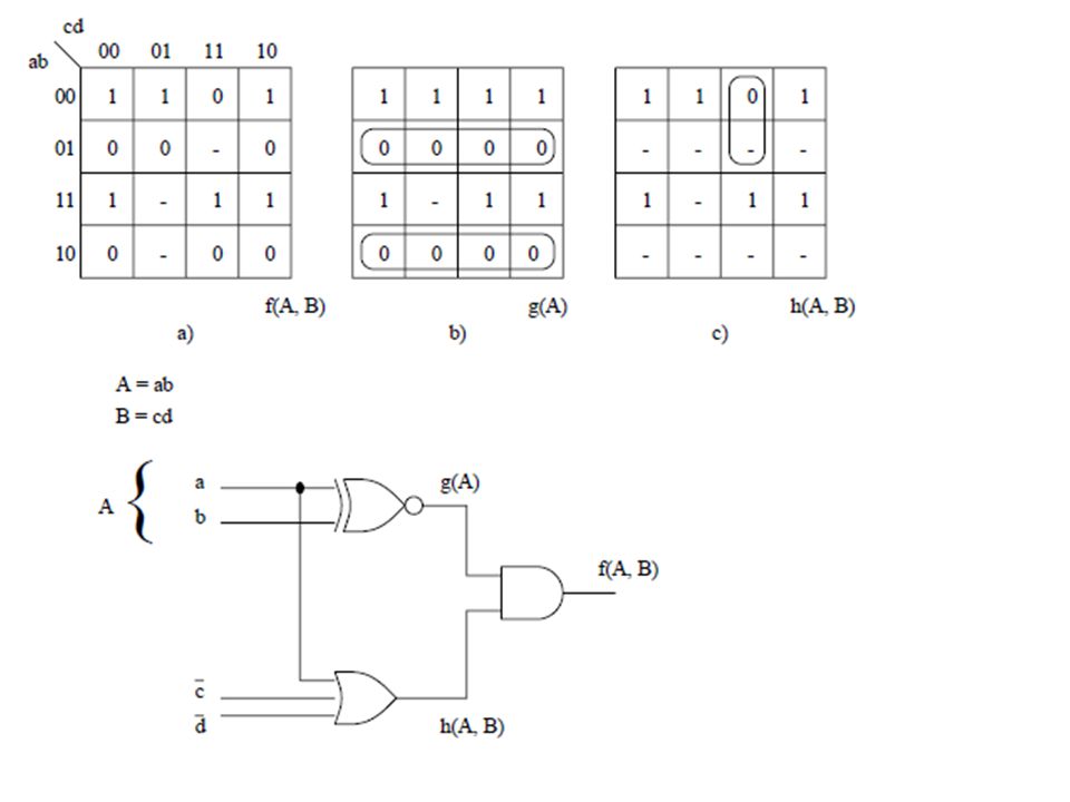
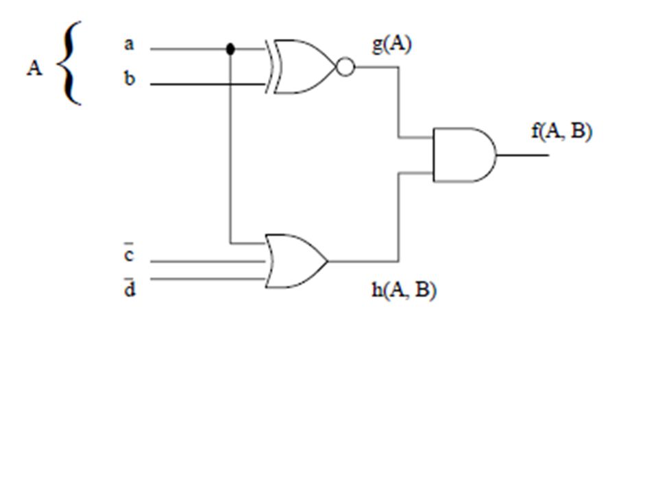
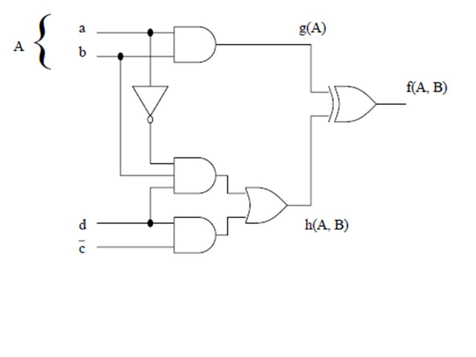
21
In this approach, the logic state is represented as resistance, where a high resistance is logical state zero, and a low resistance is logical state one. An example of this approach, the IMPLY logic gate, is shown in Figure 2.

22
Using the Memristor to build basic logic gates NOT OR AND NAND NOR EXOR MUX Memristor A B x ABX 001 011 100 111

23
Costs of gates with memristors Realized with memristors Numbers of levels IMPLY11+ AND33 OR22+ NAND22+ NOR33 EXOR43 XNOR INHIBIT22+ NOT11+ MUX53 Good for TANT, Negative gate methods CHANGE

24
examples ((abc)’+ (ab))’ + (bcd) = ((a’ + b’ + c’) + ab)’ + bcd = (abc) * (ab)’ + bcd = (abc) * (a’ + b’) + bcd = (b’c) + bcd
’+ (ab))’ + (bcd) = ((a’ + b’ + c’) + ab)’ + bcd = (abc) * (ab)’ + bcd = (abc) * (a’ + b’) + bcd = (b’c) + bcd")
25
example ((ab) 0) = (a’+b’) ((ab) (ab)) = (a’+b’) + ab (0 ab) = (ab) (a b) = (a’+b)
 0) = (a’+b’) ((ab) (ab)) = (a’+b’) + ab (0 ab) = (ab) (a b) = (a’+b)")
26
a b a + b a a b a + b a 0 a b ( a + b) = a * b 0 a a + b = (a * b) b 0 All these circuits assume that value of b already exists. If it does not exist, we need two inverters (from IMPLY) to create it.
 to create it..")
27
a b a + b a a b a + b a 0 a b ( a + b) = a * b 0 a (a * b) b 0 0 All these circuits assume that value of b already exists. If it does not exist, we need two inverters (from IMPLY) to create it.
 to create it..")
28
Now we assume that all inputs must be created with Stateful IMPLY technology from scratch.

29
NOT & OR

30
NOTOR with two inputs A 0 B x A B x A 0 x Ax B 0 0

31
NOT A 0 x Ax B C A 0 NOT is a one WM gate AAAA

32
B 2-input OR is a two WM gate A 0 B X=A+B B 0 0 A+B BBBB 0 B 2-input OR A B 0 AAAA 0 0

33
NAND & AND

34
NAND A 0 B x A B x NAND & AND

35
B C A 0 0 2-input AND is a two ancilla gate 2-input NAND is a one ancilla gate 0 NAND(a,b) AND(a,b) 0 NAND & AND
 AND(a,b) 0 NAND & AND")
36
0 b c d Working (memorizing) memristor (b a) =b’+a (c (b a) c) = (c’+(b’+a)=(bc)’+a (bcd)’+0 0 y z v (yzv)’ + 0 0 Realization of a Sum of positive Products bcd+yzv Imply serves as inverter NAND(b,c,d) NAND(y,z,v) 1 2 1 2 Two Working Memristors SOP
 memristor (b a) =b’+a (c (b a) c) = (c’+(b’+a)=(bc)’+a (bcd)’+0 0 y z v (yzv)’ Realization of a Sum of positive Products bcd+yzv Imply serves as inverter NAND(b,c,d) NAND(y,z,v) Two Working Memristors SOP")
37
Inhibit gate A * B’ = (A’ + B)’ 2 gates B C A 0 0 2-input INHIBIT is a two WM gate A’ Two working bits B’ A’ + B 0 A * B’ = (A’ + B)’
’ 2 gates B C A input INHIBIT is a two WM gate A’ Two working bits B’ A’ + B 0 A * B’ = (A’ + B)’")
38
PSE gates

39
B C A AA 0 0 PS is a two WM gate 0 0 X=(AB)’C (AB) (AB) + C’ (AB)’
’C (AB) (AB) + C’ (AB)’")
40
A B C D E F B C A 0 (A+B+C)=X D 0 X’+D’+E’+F’= (XDEF)’ E F AA 00 BB CC X XDEF X= (A+B+C) 0 0 PSE gate has 2 WM
=X D 0 X’+D’+E’+F’= (XDEF)’ E F AA 00 BB CC X XDEF X= (A+B+C) 0 0 PSE gate has 2 WM")
41
NOR Gates

42
NOR B C A AA 0 0 0 NOR is a two WM bit gate A A+B BB 0 (A+B)’
’")
43
EXOR Gates

44
EXOR = 8 literals in NAND = 8 IMPLY B A 0 EXOR is a three WM gate 0 A’B + A B’ A’ A’ B’ B A A A + B’ 0 A’B 0 B’ B B + A’ 0

45
SYNTHESIS WITH EXORS WITH NO LIMIT ON NUMBER OF ANCILLA BITS

46
B A0 0 A’B + A B’ A’ A A + B’ 0 A’B 0B’ B B + A’ 0 C 0 0 A’B + A B’ A’ A A + B’ 0 A’B 0B’ B B + A’ 0 First Working Memristor Second Working Memristor Third Working Memristor Fourth Working Memristor This circuit has 4 working memristors and 16 IMPLY gates

47
B A 0 0 A’B + A B’ A’ A A + B’ 0 A’B 0 B’ B B + A’ 0

48
MUX

49
MUX B 0 MUX is a three ancilla gate 0 A C (AB)’ AB + A’C A A’ B C (A’C)’ 0 0 A’ A (A+C’)’ 7 WM expected
’ AB + A’C A A’ B C (A’C)’ 0 0 A’ A (A+C’)’ 7 WM expected")
50
Circuits from reversible gates versus circuits from memristor material implications Similarities No fanout In-gate memory exists Differences No inverter Different gates

51
Examples of typical multi- input gates

52
B 0 C A AA A + B A + B + C = (ABC) Realization of positive product (negated) which is multi-input NAND
 Realization of positive product (negated) which is multi-input NAND")
53
0 A A A + BA + B + C Realization of positive product (negated) which is multi-input OR AAAA BBBB CCCC
 which is multi-input OR AAAA BBBB CCCC")
54
Gates from AND and OR similar to PS Gate

55
(A+B+C) DE A B C D E A B C D E D’ + E’ + (ABC) PSE gate with not negated inputs TANT IMPLICANT DE * (A+B+C) Various gates similar to PSE
 DE A B C D E A B C D E D’ + E’ + (ABC) PSE gate with not negated inputs TANT IMPLICANT DE * (A+B+C) Various gates similar to PSE")
56
B C A AA A + B (ABC) 0 D 0 0 E D + E= (DE) (ABC) We loose info and initialize to zero DE + (ABC) Sum of any number of positive products is a two-ancilla gate
 0 D 0 0 E D + E= (DE) (ABC) We loose info and initialize to zero DE + (ABC) Sum of any number of positive products is a two-ancilla gate")
57
AND/OR gate (PS gate)
")
58
A B C D E F A B C D E F A B C D E F A+B+C

59
METHOD 1: Example of synthesis using the step-by- step realization method with KMaps

60
Using the Memristor to build OTHER gates

61
Example of synthesis based on mapping Mapping from an existing circuit network Can be solved using dynamic programming

62
MATERIAL NOT FOR NOW Slides below have errors

63
Ashenhurst Curtis Decomposition

64
Ashenhurst-Curtis Decomposition arbitrary

65
Ashenhurst-Curtis Decomposition with symmetric predecessor arbitrary symmetric

66
Ashenhurst-Curtis Decomposition with symmetric predecessor symmetric Arbitrary remainder

67
Ashenhurst-Curtis Decomposition with symmetric predecessor and successor symmetric

68
METHOD 2: Bi-Decomposition of Binary Single-Output Circuits

69
Boolean Operations

70
Graphical OR decomposition 1.We arbitrarily partitionate all input variables to sets {a,b} and {c,d} 2.We assume OR gate 3. We find function g on variables a and b only 4. We calculate the reminder function g on variables c and d and may be more

71
First variant of synthesis Student should show how this function is realized on memristors to minimize the number of working transistors (Ancilla)
")
72
Second variant of synthesis We assume AND Decomposition

78
Our final algorithm (initial ideas) 1.Use METHOD 2 - bi-decomposition, first try OR decomposition, next AND, next EXOR. 2.Count width of circuit at every stage. 3.If the desired width is exceeded continue function using METHOD 1. 1.Anika, give examples of combined method on function of 5 variables or 6 variables. 2. Write the pseudo-code of the final algorithm before programming.

79
The method to analyze all circuits in bi- decomposition, and how to realize them with memristors

80
\/ * \/ \/ * * \/ + \/ Or \/ * \/ \/ * \/ \/ + \/ IMPLY NAND IMPLY NAND X Y NOT X Y’ X Y ZV exor X Y Z’ V

81
+ * \/ + * * + + + + * \/ + * * + + + exor Please complete

82
+ * \/ + * * + + + + * \/ + * * + + + exor Please complete

83
+ * * + + + + * * * * * * * *

84
+ * * + + + + * * * * * * * * Can we evaluate quickly how many two-input NAND and IMPLY gates and how many ancilla we need directly from a tree? a b cd e f g h i j k l m n p r

85
+ * * + + + + a b c d g h i k

86
+ * * + + + + a b c d g h i k C EXOR B A 0 EXOR(A,B) 0 B A 0 EXOR(A,B) a h b c d g k i a+b 0 c+d g+h i+k
 0 B A 0 EXOR(A,B) a h b c d g k i a+b 0 c+d g+h i+k")
87
Memristors vs reversible a b c d Working (memorizing) memristor (a b) = a’+b ((a b) c) = (a’+b)’+c)=(ab’+c) (((a b) c) d) =( (ab’+c) d) = ((ab’)+c)’ +d =(ab’)’ * c’ + d = = (a’+b)c’+d= =a’c’ + bc’ + d
 memristor (a b) = a’+b ((a b) c) = (a’+b)’+c)=(ab’+c) (((a b) c) d) =( (ab’+c) d) = ((ab’)+c)’ +d =(ab’)’ * c’ + d = = (a’+b)c’+d= =a’c’ + bc’ + d")
88
a=0 b c d (a b) = a’+b ((a b) c) = (a’+b)’+c)=(ab’+c) (((a b) c) d) =( (ab’+c) d) = ((ab’)+c)’ +d =(ab’)’ * c’ + d = = (a’+b)c’+d= =a’c’ + bc’ + d Example of circuit synthesis with negations along the bit line =0’c’ + bc’ + d
 = a’+b ((a b) c) = (a’+b)’+c)=(ab’+c) (((a b) c) d) =( (ab’+c) d) = ((ab’)+c)’ +d =(ab’)’ * c’ + d = = (a’+b)c’+d= =a’c’ + bc’ + d Example of circuit synthesis with negations along the bit line =0’c’ + bc’ + d")
89
a b c d (a b) = a’+b ((a b) c) = (a’+b)’+c)=(ab’+c) (((a b) c) d) =( (ab’+c) d) = ((ab’)+c)’ +d =(ab’)’ * c’ + d = = (a’+b)c’+d= =a’c’ + bc’ + d The same circuit in my new notation 1 2 1 2 1 2 Working bits
 = a’+b ((a b) c) = (a’+b)’+c)=(ab’+c) (((a b) c) d) =( (ab’+c) d) = ((ab’)+c)’ +d =(ab’)’ * c’ + d = = (a’+b)c’+d= =a’c’ + bc’ + d The same circuit in my new notation Working bits")
90
a b c d (a b) = a’+b ((a b) c) = (a’+b)’+c)=(ab’+c) (((a b) c) d) =( (ab’+c) d) = ((ab’)+c)’ +d =(ab’)’ * c’ + d = = (a’+b)c’+d= =a’c’ + bc’ + d 1110 1110 1110 0110 1--0 1--0 1--0 0--0 0--1 0--1 0--1 1--1 1 1 1 0 d c b Graphical Illustration of the method with negations in the bit line
 = a’+b ((a b) c) = (a’+b)’+c)=(ab’+c) (((a b) c) d) =( (ab’+c) d) = ((ab’)+c)’ +d =(ab’)’ * c’ + d = = (a’+b)c’+d= =a’c’ + bc’ + d d c b Graphical Illustration of the method with negations in the bit line")
91
p mi p = p + mi 0 mi 0 mj mi S1 S2 S3 mj 0 mi

92
AND/OR A 0 B X=(AB)’ A B x 0 C 0 C D X=(AB)’C A 0 B X=(AB)’ 0 C 0 X=(AB)’C = (A’+B’)C X=AB X=AB+C’
’ A B x 0 C 0 C D X=(AB)’C A 0 B X=(AB)’ 0 C 0 X=(AB)’C = (A’+B’)C X=AB X=AB+C’")
93
MUX A C B 0 A B C 0 (A’B)+(AC) (A+C’)’= A’C A’+B’ = (AB)’ AB +A’C
+(AC) (A+C’)’= A’C A’+B’ = (AB)’ AB +A’C")
94
MUX B 0 MUX is a three ancilla gate 0 MUX A C 0 0 A B C X X Can we build a less expensive MUX?

95
10 01 a01a01 b 0 1 10 01 a01a01 Realize best positive product 10 0- a01a01 b 0 1 Create the reminder function Invert the remainder function 01 1- a01a01 b 0 1 Realize best positive product 01 1- a01a01 b 0 1 0- 1- a01a01 Create the reminder function Invert the remainder function 1- 0- a01a01 b 0 1 There are no positive products so invert 0- 1- a01a01 b 0 1 a b out 0 aa a* b = X a* b + ab Simplified schematics for AB + X Simplified schematics for inverter

96
a b out 0 aa a* b a* b + ab a+b (AB)’ (AB) inverter 0 Real Circuit for the last example, showing all details
’ (AB) inverter 0 Real Circuit for the last example, showing all details")
97
A B 0 0 B A 0 C 0 C Three input EXOR is a Three Ancilla Gate

98
SYNTHESIS WITH EXORS WITH NO LIMIT ON NUMBER OF ANCILLA BITS A B 0 C 0

99
1.In their design there are 21 memristors 2.We need 2 two-input exors. Exor has 4 gates. 3.2*4 = 8. Our design has 8 gates not 21. 4.But we have fan-out of two A B 0 C Conclusion. When we want to decrease the number of ancilla bits we need: Conclusion. When we want to decrease the number of ancilla bits we need: 1.Methods with many exors are not good as they would require copying elements. 2.Methods are good if they naturally create trees 0

100
A B 0 C C 0 A B 0 1.But we have fan-out of two 2.So we replicate the first EXOR, and we have only 12 gates, not 21 as in their design Can we design three-input EXOR as a two-ancilla gate?

101
A B 0 C C A B 0 Synthesis with copying to get a tree 0 A XOR B

102
C EXOR B A0 EXOR(A,B) 0 Example of coloring to show that exor of three inputs must have three ancilla, all in red are one ancilla but blue and green cannot be combined
 0 Example of coloring to show that exor of three inputs must have three ancilla, all in red are one ancilla but blue and green cannot be combined")
103
C EXOR B A0 EXOR(A,B) 0 B A0 EXOR(A,B)
 0 B A0 EXOR(A,B)")
Similar presentations


 (Karnaugh Map)>")


 1 Feb Learning Objectives>")