Download presentation
Presentation is loading. Please wait.

1
JFET &MOSFET PREPARED BY JAYSWAL JAYDEEP (150403111005) GOHIL DARSHAN (150403111004) PARMAR NARESH (150403111007) THAKOR MAHESH (150403111015) Guided By Prof. Rahul G.Patel Department of Electronics and Communication Engineering, Sankalchand Patel College Of Engineering, Visnagar

2
Junction Field Effect Transistor There Are Two Types Of JFET:- (1)n-channel JFET (2)p-channel JFET
n-channel JFET (2)p-channel JFET")
3
JFET CONSTRUCTION There are three terminals: Drain (D) and Source (S) are connected to n-channel Gate (G) is connected to the p-type material
 and Source (S) are connected to n-channel Gate (G) is connected to the p-type material")
4
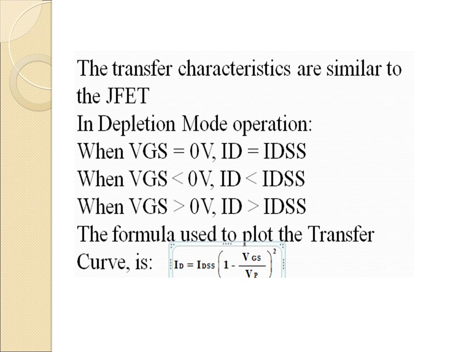
JFET Operating Characteristics There are three basic operating conditions for a JFET: JFET’s operate in the depletion mode only A.VGS = 0, VDS is a minimum value depending on IDSS and the drain and source resistance B.VGS < 0, VDS at some positive value and C.Device is operating as a Voltage-Controlled Resistor For an n channel JFET, VGS may never be positive* For an p channel JFET, VGS may never be negative *

5
Transfer Characteristics The input-output transfer characteristic of the JFET is not as straight forward as it is for the BJT In a BJT, (hFE) defined the relationship between I B (input current) and I C (output current). In a JFET, the relationship (Shockley’s Equation) between V GS (input voltage) and I D (output current) is used to define the transfer characteristics, and a little more complicated (and not linear):
 between V GS (input voltage) and I D (output current) is used to define the transfer characteristics, and a little more complicated (and not linear):.")
6
N-Channel JFET Operation

7
N-Channel JFET Symbol

8
Saturation Point At the pinch-off point: any further increase in V GS does not produce any increase in I D. V GS at pinch-off is denoted as Vp. ID is at saturation or maximum. It is referred to as I DSS. The ohmic value of the channel is at maximum.

9
P-channel JFET p-Channel JFET operates in a similar manner as the n-channel JFET except the voltage polarities and current directions are reversed

10
P-channel JFET Characteristics As VGS increases more positively the depletion zone increases I D decreases (I D < I DSS ) eventually I D = 0A Also note that at high levels of VDS the JFET reaches a breakdown situation. ID increases uncontrollably if V DS > V DSmax.

11
MOSFET

12
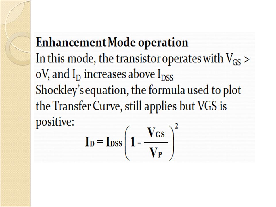
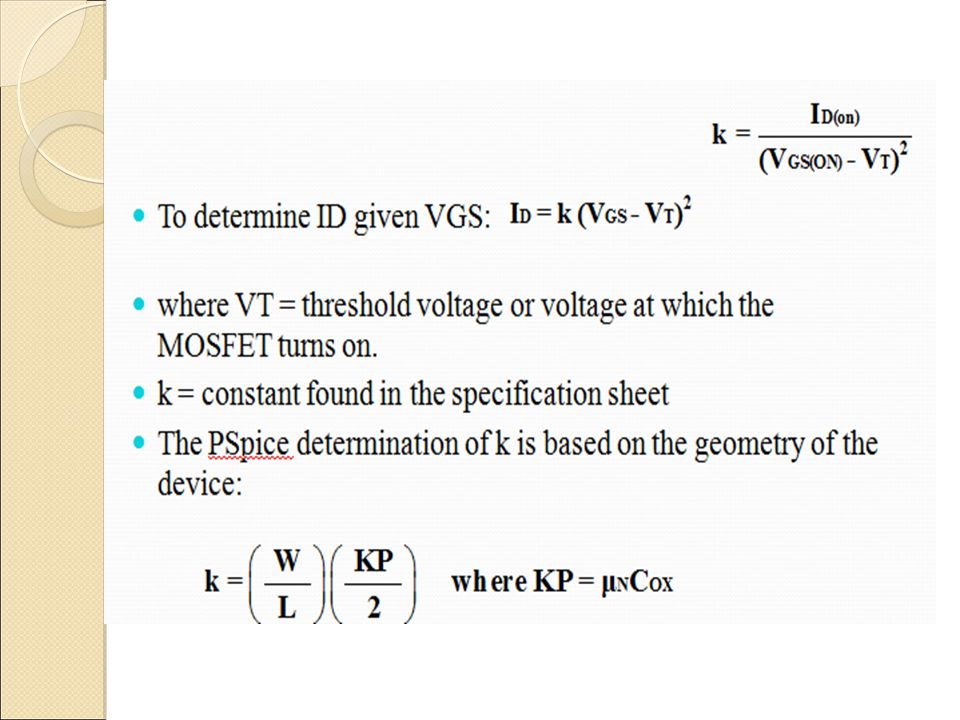
MOSFETs have characteristics similar to JFETs and additional characteristics that make then very useful. Let’s see more details in MOSFET. There are 2 types of MOSFET’s: Depletion mode MOSFET (D-MOSFET) Operates in Depletion mode the same way as a JFET when VGS 0 Operates in Enhancement mode like E-MOSFET when VGS > 0 Enhancement Mode MOSFET (E-MOSFET) Operates in Enhancement mode IDSS = 0 until VGS > VT (threshold voltage)
 Operates in Depletion mode the same way as a JFET when VGS 0 Operates in Enhancement mode like E-MOSFET when VGS > 0 Enhancement Mode MOSFET (E-MOSFET) Operates in Enhancement mode IDSS = 0 until VGS > VT (threshold voltage).")
13
MOSFET HANDALING MOSFETs are very static sensitive. Because of the very thin SiO 2 layer between the external terminals and the layers of the device, any small electrical discharge can stablish an unwanted conduction. Protection: Always transport in a static sensitive bag Always wear a static strap when handling MOSFETS Apply voltage limiting devices between the Gate and Source, such as back-to- back Zeners to limit any transient voltage

14
D-MOSFET Symbols

15
Construction of D-MOSFET The Drain (D) and Source (S) leads connect to the to n-doped regions.These N-doped regions are connected via an n-channel This n-channel is connected to the Gate (G) via a thin insulating layer of SiO 2 The n-doped material lies on a p-doped substrate that may have an additional terminal connection called SS
 and Source (S) leads connect to the to n-doped regions.These N-doped regions are connected via an n-channel This n-channel is connected to the Gate (G) via a thin insulating layer of SiO 2 The n-doped material lies on a p-doped substrate that may have an additional terminal connection called SS")
16
Basic Operation:-

18
D-MOSFET ENHENCEMENT MODE OPERATION:-

20
P-Channel Depletion Mode:-

21
The p-channel Depletion mode MOSFET is similar to the n-channel except that the voltage polarities and current directions are reversed

22
Enhancement Mode MOSFET’s

23
The Drain (D) and Source (S) connect to the to n-doped regions These n-doped regions are not connected via an n- channel without an external voltage The Gate (G) connects to the p-doped substrate via a thin insulating layer of SiO 2 The n-doped material lies on a p-doped substrate that may have an additional terminal connection called SS
 and Source (S) connect to the to n-doped regions These n-doped regions are not connected via an n- channel without an external voltage The Gate (G) connects to the p-doped substrate via a thin insulating layer of SiO 2 The n-doped material lies on a p-doped substrate that may have an additional terminal connection called SS")
24
E-MOSFET Symbols

25
Basic Operation :-

26
VGS is always positive IDSS = 0 when VGS < VT As VGS increases above VT, ID increases If VGS is kept constant and VDS is increased, then ID saturates (IDSS) The saturation level, VDSsat is reached.
 The saturation level, VDSsat is reached.")
27
Transfer Curve

29
p-Channel Enhancement Mode MOSFETs

30
A.Abhari CPS213 1.www.slideshare.com 2.www.elprojects.blog.com 3.www.scs.ryerson.com Reference

31
THANK YOU

Similar presentations


>")
 Chapter 7. JFET VGS Effect G-S junction is reverse-biased with negative voltage (VG) depletion region VG less than.>")
>")
 Importance for LSI/VLSI –Low fabrication cost –Small size –Low power consumption Applications –Microprocessors –Memories.>")


>")
 by:- Uttampreet Singh Lecturer-Electrical Engg. Govt. Polytechnic College, G.T.B.garh, Moga.>")
 –3 layers of doped semiconductor –2 p-n junctions –Layers.>")


>")
