Download presentation
Presentation is loading. Please wait.

1
3PNT – Photonics and Nanotechnology Part I Quantum electronic and optical confinement (6 lectures, Prof BN Murdin) –Recap of basic semiconductor physics –Semiconductor quantum structures Wells, wires, dots –Photonic bandgap structures –Fabrication of nanostructures Part II Advanced Lasers and optical communications (6 lectures, Dr SJ Sweeney) –Semiconductor lasers –Optical amplifiers –Optical fibres –Telecommunications Part III Modern Nanophotonics (8 lectures, Profs J Allam and BN Murdin) –Including: Spintronics Microcavities Polymer photonic devices Biophotonics
 –Recap of basic semiconductor physics –Semiconductor quantum structures Wells, wires, dots –Photonic bandgap structures –Fabrication of nanostructures Part II Advanced Lasers and optical communications (6 lectures, Dr SJ Sweeney) –Semiconductor lasers –Optical amplifiers –Optical fibres –Telecommunications Part III Modern Nanophotonics (8 lectures, Profs J Allam and BN Murdin) –Including: Spintronics Microcavities Polymer photonic devices Biophotonics")
2
Take a strip off the bottom of a piece of A4 paper and cut it in half, then half again….. N o CutsLengthObjects on that scale 021.0 cm 25.25 cm 41.31 cm 63.28 mm 8 820 m 10 205 m 12 51.2 m 14 12.8 m 16 3.2 m 18801 nm 20200 nm 2250.0 nm 2412.5 nm 263.13 nm 287.82 Å Red blood cell Diameter of a human hair Bacteria Thickness of a cell wall Toothpick Cluster of atoms, a nanoparticle Pencil Diameter of a finger Eight hydrogen atoms lined up Kernel of corn Silt Gnat Resolution of optical microscope Virus, Intel’s smallest transistor Tip of a needle, bee sting

3
Take a strip off the bottom of a piece of A4 paper and cut it in half, then half again….. N o Cuts LengthObjects on that scale 021.0 cm 25.25 cm 41.31 cm 63.28 mm 8 820 m 10 205 m 12 51.2 m 14 12.8 m 16 3.2 m 18801 nm 20200 nm 2250.0 nm 2412.5 nm 263.13 nm 287.82 Å Objects on that scale Pencil Toothpick Diameter of a finger Kernel of corn Gnat Tip of a needle, bee sting Diameter of a human hair Silt Red blood cell Bacteria Resolution of optical microscope Virus, Intel’s smallest transistor Thickness of a cell wall Cluster of atoms, a nanoparticle Eight hydrogen atoms lined up

4
Nanophotonics: Nobel Prizes in Physics 1991 & 2000 2000 ZI Alferov Russia, H Kroemer, Germany, JS Kilby USA for the invention of integrated circuit, and for developing semiconductor heterostructures, including: –The heterojunction laser 1991 PG de Gennes, France for generalizing the theory of order/disorder in simple systems (e.g. magnets) to complex forms of matter, in particular: –Liquid crystals
 to complex forms of matter, in particular: –Liquid crystals.")
5
Other nanotechnology Nobel prizes 1973 tunnelling phenomena –L Esaki Japan, I Giaever USA (b. Norway) BD Josephson United Kingdom 1985 quantum Hall effect –K von Klitzing Germany 1986 electron microscope –E Ruska, G Binnig, Germany and H Rohrer, Switzerland
 BD Josephson United Kingdom 1985 quantum Hall effect –K von Klitzing Germany 1986 electron microscope –E Ruska, G Binnig, Germany and H Rohrer, Switzerland.")
6
Other photonics Nobel prizes 1964 the maser/laser –CH Townes USA, NG Basov USSR, AM Prokhorov USSR 1971 holography –D Gabor, United Kingdom (b. Hungary) 1981 laser and electron spectroscopy –N Bloembergen USA (b Netherlands), AL Schawlow USA, KM Siegbahn Sweden 2005 quantum theory of optical coherence and laser-based precision spectroscopy –RJ Glauber USA, JL Hall USA, TW Hänsch Germany
 1981 laser and electron spectroscopy –N Bloembergen USA (b Netherlands), AL Schawlow USA, KM Siegbahn Sweden 2005 quantum theory of optical coherence and laser-based precision spectroscopy –RJ Glauber USA, JL Hall USA, TW Hänsch Germany.")
7
Challenges for Nanotechnology Nanomanufacturing –Incorporating nanoscale materials into larger scale devices (e.g. heterostructure lasers) –Designing materials with nanoscale structure (e.g. synthetic opals) –Nanomachines (microcraft and robotics) Nanophysics –Investigation of Nano-Electronics, -Photonics, and -Magnetics Nanotechnology applications –Detection of chemical-biological-radiological-medical compounds –Therapeutics (e.g. drug delivery) –Instrumentation, and Metrology (e.g. gyros) –Energy Conversion (e.g. solar cells, suncream) and storage (e.g. zeolytes) –Processes for environmental improvement
 –Designing materials with nanoscale structure (e.g. synthetic opals) –Nanomachines (microcraft and robotics) Nanophysics –Investigation of Nano-Electronics, -Photonics, and -Magnetics Nanotechnology applications –Detection of chemical-biological-radiological-medical compounds –Therapeutics (e.g. drug delivery) –Instrumentation, and Metrology (e.g. gyros) –Energy Conversion (e.g. solar cells, suncream) and storage (e.g. zeolytes) –Processes for environmental improvement.")
8
Current photonics industries Products in the Growing Period: commercially available technology and expanding market scale –TFT-LCD (TV, Monitor), PDP –DVD Player (Audio, Video),CD/DVD Recorder (Burner), Discs –Imaging devices (DSC, image sensor) Products in the Emerging Period: technology under development with high market potential –Organic-EL, high brightness LED, LD –High-Density Optical Discs (bluray), LCD (LTP-Si, reflective, low power consumption), Projectors (DLP, LCoS, LCD, VR) –Advanced networking systems (Local LAN, all-optical networks)
, PDP –DVD Player (Audio, Video),CD/DVD Recorder (Burner), Discs –Imaging devices (DSC, image sensor) Products in the Emerging Period: technology under development with high market potential –Organic-EL, high brightness LED, LD –High-Density Optical Discs (bluray), LCD (LTP-Si, reflective, low power consumption), Projectors (DLP, LCoS, LCD, VR) –Advanced networking systems (Local LAN, all-optical networks)")
9
Overview of global photonics market

10
What is Nano-Photonics? Information technology: storage and processing (Moore’s Law), transmission and reception, displays Sensors: identification of compounds (bio/chem/medical), nondestructive testing and evaluation Nanomedicine: microscopy, disease detection and treatments Power generation and efficient utilization: solar cells, Thermo-photovoltaics (TPVs), lasers, LED lighting
, transmission and reception, displays Sensors: identification of compounds (bio/chem/medical), nondestructive testing and evaluation Nanomedicine: microscopy, disease detection and treatments Power generation and efficient utilization: solar cells, Thermo-photovoltaics (TPVs), lasers, LED lighting.")
11
What’s So Great About Semiconductors? The resistance of a semiconductor structure may be fixed within a range of many orders of magnitude by various means: –Impurities (doping), homostructure design, heterostructure design etc…. Once produced, the resistance of the structure my then also be varied over a range of many orders of magnitude by various means: –Light, electric field, current, temperature, magnetic fields, etc… Photo-Diodes Resistance = f(incident light) Transistors Resistance = f(V) or f(I) Thermo-resistors Resistance = f(Temperatur) Finally, semiconductors can actively produce, modulate, switch and recolour light beams, and are the basis of a huge variety of useful “photonic” devices.
, homostructure design, heterostructure design etc…. Once produced, the resistance of the structure my then also be varied over a range of many orders of magnitude by various means: –Light, electric field, current, temperature, magnetic fields, etc… Photo-Diodes Resistance = f(incident light) Transistors Resistance = f(V) or f(I) Thermo-resistors Resistance = f(Temperatur) Finally, semiconductors can actively produce, modulate, switch and recolour light beams, and are the basis of a huge variety of useful photonic devices..")
12
Things that can’t be made from Si Light emitters and optical modulators (it’s “indirect”) –Light emitting diodes, Laser diodes (any wavelength) –Amplitude modulation of light for fibre telecoms Mid-IR, far-IR, UV detectors (interband absorption is 0.5 to1.1 μm) –Fibre communication receivers ( = 1.3 and 1.55 μm) –Atmospheric “windows” ( = 3 to 5 μm and 8 to 12 μm) –Infrared imaging arrays (responding to 500 K black bodies) –Solar blind detectors ( ≤ 0.5 μm) –Efficient solar cells Very-high speed electronics (its “effective mass” is high) –Operating at 40 GHz and above for mobile phones and fibre telecoms High temperature electronics (bandgap and melting point too low) –Operable at temperatures above 200˚C for process monitoring
 –Light emitting diodes, Laser diodes (any wavelength) –Amplitude modulation of light for fibre telecoms Mid-IR, far-IR, UV detectors (interband absorption is 0.5 to1.1 μm) –Fibre communication receivers ( = 1.3 and 1.55 μm) –Atmospheric windows ( = 3 to 5 μm and 8 to 12 μm) –Infrared imaging arrays (responding to 500 K black bodies) –Solar blind detectors ( ≤ 0.5 μm) –Efficient solar cells Very-high speed electronics (its effective mass is high) –Operating at 40 GHz and above for mobile phones and fibre telecoms High temperature electronics (bandgap and melting point too low) –Operable at temperatures above 200˚C for process monitoring")
13
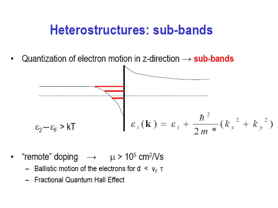
What is a heterostructure ? A device built from different semiconductor materials, thus exploiting the differences in electronic level structure.

14
Ohm’s Law for grown-ups The response (j) to the drive (F) is a material property ( ), which is independent of size and determined by the number of mobile charges, and the charge and the “mobility” of each. MetalsemicondInsulator ( -1 m -1 ) >10 6 10 5 -10 -7 <10 -8 n (m -3 )10 28 10 27 -10 16 <10 15 (mV -1 s -1 ) 10 -3 10 -3 -10 2
 > <10 -8 n (m -3 ) <10 15 (mV -1 s -1 )")
15
Why such big variation in ? Metal –Continuous DoS n ≠ n(T) –Drude mobility: = e (T)/m –Temp. dep. of comes from the electron scattering time Semiconductor –DoS has gap n = n(E F,T) depends very sensitively on both on doping and temperature EFEF f Fermi occupation function In the metal the charges that can take part in the transport are all those near E F. This number is not very sensitive to T. In the semiconductor most states near E F are missing, and the occupation of the remainder is very sensitive to T. E
 depends very sensitively on both on doping and temperature EFEF f Fermi occupation function In the metal the charges that can take part in the transport are all those near E F. This number is not very sensitive to T. In the semiconductor most states near E F are missing, and the occupation of the remainder is very sensitive to T. E.")
16
How do we control n? The Fermi level (or chemical potential) of the electrons falls in a gap of the band structure. Doping allows us to control the position of E F in the gap. –Either electrons (n-type) or holes (p-type) act as carriers of charge. We can also optically excite electron-hole pairs. How do we calculate n? This requires knowing the Density of States (DoS) – see homework.
 of the electrons falls in a gap of the band structure. Doping allows us to control the position of E F in the gap. –Either electrons (n-type) or holes (p-type) act as carriers of charge. We can also optically excite electron-hole pairs. How do we calculate n. This requires knowing the Density of States (DoS) – see homework..")
17
Schroedinger Eqn in 1D Schrodinger’s Equation… … the energy of a state is related to the curvature of the wavefunction Tighter confinement → Higher Energy Nodes in wavefunction → Higher Energy Fixed box boundary conditions give standing waves Periodic b.c.’s allow travelling waves Ψ(z) Ψ 2 (z) n=1 n=2 n=3 z/L E
 Ψ 2 (z) n=1 n=2 n=3 z/L E")
18
Energy bands for 1-D, one atom lattice 1D, one atom basis: each s & p forms one band. –Two atom basis: each s & p forms two bands. –3D: p-orbitals are 3-fold degenerate, p x, p y, p z.

19
Crystal structure of GaAs FCC lattice with two atom basis: 1 Ga & 1 As atom per lattice site –Tetrahedrally coordinated –Ga: [Ar] 3d 10 4s 2 4p 1 –As: [Ar] 3d 10 4s 2 4p 3 –3 valence e - per gallium atom –5 valence e - per arsenic atom Germanium: –Both sites still different (different coordination) but both atoms same species –Ge: [Ar] 3d 10 4s 2 4p 2 total: 8 valence e - per unit cell –4 bands full (x2 for spin)
![Crystal structure of GaAs FCC lattice with two atom basis: 1 Ga & 1 As atom per lattice site –Tetrahedrally coordinated –Ga: [Ar] 3d 10 4s 2 4p 1 –As: [Ar] 3d 10 4s 2 4p 3 –3 valence e - per gallium atom –5 valence e - per arsenic atom Germanium: –Both sites still different (different coordination) but both atoms same species –Ge: [Ar] 3d 10 4s 2 4p 2 total: 8 valence e - per unit cell –4 bands full (x2 for spin)](http://images.slideplayer.com/47/11673198/slides/slide_19.jpg "Crystal structure of GaAs FCC lattice with two atom basis: 1 Ga & 1 As atom per lattice site –Tetrahedrally coordinated –Ga: [Ar] 3d 10 4s 2 4p 1 –As: [Ar] 3d 10 4s 2 4p 3 –3 valence e - per gallium atom –5 valence e - per arsenic atom Germanium: –Both sites still different (different coordination) but both atoms same species –Ge: [Ar] 3d 10 4s 2 4p 2 total: 8 valence e - per unit cell –4 bands full (x2 for spin)")
20
Bandstructure of GaAs L-valley 111 X-valley 100 wavevector, k Energy (eV) Empty conduction bands -valley 000 EFEF Full valence bands 4p 2 4s 2 Anti-bonding Bonding Isolated atom Two atoms Two atom lattice L X kyky kXkX kzkz
 Empty conduction bands -valley 000 EFEF Full valence bands 4p 2 4s 2 Anti-bonding Bonding Isolated atom Two atoms Two atom lattice L X kyky kXkX kzkz")
21
Effective mass For almost all properties of semiconductors the most important states are the ones near the band edges, because that’s where the electrons and holes collect. The bottom of the conduction band is a turning point, so odd k terms are zero : We (usually) neglect higher terms (small k, small E), so we write: Electrons move as if in free space, but with a mass determined by curvature: the "effective mass". E k
 neglect higher terms (small k, small E), so we write: Electrons move as if in free space, but with a mass determined by curvature: the effective mass . E k .")
22
Optical transitions Interband transitions Intraband transitions nanoseconds in GaAs n-type p-type < ps in GaAs

23
Direct and indirect gap transitions h E k Direct bandgap Indirect bandgap h phonon-assisted absorption ~10 4 cm -1 ~10 2 cm -1 valley is lowest optical transitions are direct ~zero momentum transfer optical absorption length ~ 1 m X or L valley is lowest optical transitions are indirect momentum supplied by phonon optical absorption length ~ 100 m

24
E k Conduction band Valence band m c =0.07 m e, m v >>m e E G = 1.5eV GaAs EgEg Photons carry virtually no momentum Q: how much is k for absorption in GaAs 5% above gap?

25
Bandstructure of Ge and GaAs B O In C Si Ge Sn N AlP GaAs Sb Se S Zn TeCd Hg IIIIVVVIII 2 3 4 5 6 period group larger atoms

26
Band edges and vacuum level Band edge energies –The band edge energies relative to the vacuum reference level and to each other are a property of the semiconductor –Energy gap, E G : Valence band edge to conduction band edge Fermi level –Depends additionally on doping –n-type –p-type –Work function, : Fermi level to vacuum ref. vacuum reference level EGEG 0EcEFEv0EcEFEv ee Distance, z Electron energy EGEG n-type: E F is near c.b. edge

27
Homojunctions i.e. joining two pieces of same material, different doping Isolated n- and p-type: i. Have same vacuum ref., ii. Fermi levels differ iii. Both materials neutral vacuum reference level vacuum 0EcEFEv0EcEFEv qq n-type 0EcEFEv0EcEFEv qq p-type

28
Homojunctions Electrically connected: i. Charge diffuses from high concentration to low across the boundary ii. Ionised dopants left behind change potential iii. Fermi levels shift until equal 0EcEFEv0EcEFEv qq 0EcEFEv0EcEFEv qq n-type p-type +++---

29
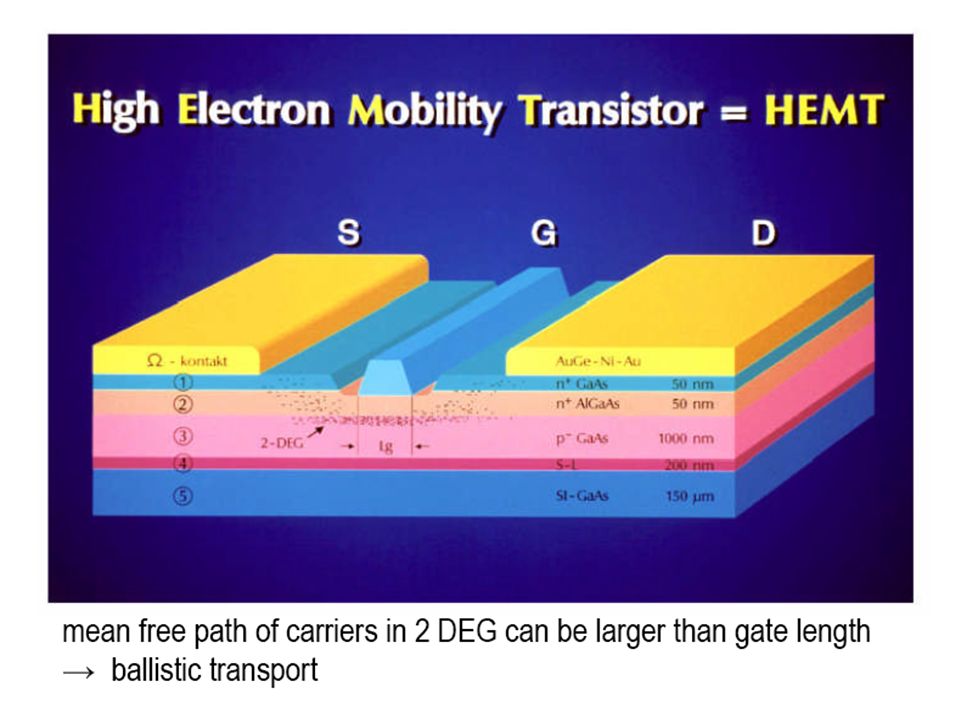
Growth of Heterostructures: Molecular Beam Epitaxy of GaAs/AlGaAs

30
Heterostructures: Bandgaps/misfits Epitaxial films may only have small lattice mismatch –the bigger the mismatch the smaller the thickness that can be grown without dislocations

31
1D P.E. landscapes: step Classically, electrons with 0 E can. Quantum mechanically, electrons with 0 E have a finite probability of being reflected by the step. Such a step can be created by laying a wide gap semiconductor on top of a narrow gap semiconductor EE E

32
Potential energy landscape model In heterojunctions electrons and holes can be modelled by the effective mass theory, even though perfect periodicity is destroyed. In this case, the potential energy profile, V(x), seen by electrons is E c (x) and that seen by holes is E v (x).
, seen by electrons is E c (x) and that seen by holes is E v (x)..")
33
Heterojunctions i.e. joining two pieces of different materials, (maybe different doping) vacuum reference level vacuum 0EcEFEv0EcEFEv qnqn n-type wide gap 0EcEFEv0EcEFEv qpqp intrinsic narrow gap
 vacuum reference level vacuum 0EcEFEv0EcEFEv qnqn n-type wide gap 0EcEFEv0EcEFEv qpqp intrinsic narrow gap.")
34
Heterojunctions Electrically connected: Discontinuity forms potential well in narrow gap material (which band depends on doping) 0EcEFEv0EcEFEv qq 0EcEFEv0EcEFEv qq n-type p-type +++ Q: draw band diagram for p-type wide gap and n-type narrow gap
 0EcEFEv0EcEFEv qq 0EcEFEv0EcEFEv qq n-type p-type +++ Q: draw band diagram for p-type wide gap and n-type narrow gap")
37
Homework Revise Density of States for 3D system (see level 2 semiconductors 2SP, level 3 Physics of Stars 3PS etc) Find out Density of states for 2D, 1D and 0D system. Bring drawings and formulas to lecture

Similar presentations


 to an empty (at T=0) conduction band look at density of states D and distribution.>")


 Low dimensional materials: Quantum wells,>")
>")
 – Energy band model – Band gap energy – Density of states – Doping Reading: Pierret 2.2-2.3, 3.1.5;>")
 Also:n 0 p 0 = n.>")


