Download presentation
Presentation is loading. Please wait.

1
Science and Technology of Nano Materials snistforum.com

2
Introduction Matter and Energy are manifestations of the universe they exist in a variety of forms and interact with each other in many ways. Nano means 10 -9. ( Nanometer is one thousand Millionth of a Meter) To understand how small one nm is let us see few comparisons 1. A Red blood cell is approximately 7000nm wide. 2. Water Molecule is almost 0.3nm across. 3. Human hair which is about 80,000nm wide. snistforum.com
 To understand how small one nm is let us see few comparisons 1. A Red blood cell is approximately 7000nm wide. 2. Water Molecule is almost 0.3nm across. 3. Human hair which is about 80,000nm wide. snistforum.com.")
3
Nano Material 1.Nano Materials could be defined as the materials with at least one of its dimensions in the range of a Nano meter. 2.Thus the material need not be so small that it cannot be seen, it can be a large surface or a long wire whose thickness is in the scale of Nanometers. 3.Materials that are Nano scale in one dimension are layers, such as a Thin films or Surface coatings. 4.Materials that are Nano Scale in two dimensions include Nano wires and Nano tubes. 5.Materials that are Nano scale in three dimensions are particles for example precipitates, colloids and quantum dots (Small particles of Semiconductor Materials) snistforum.com
 snistforum.com.")
4
Nano Science Nano Science can be defined as the study of phenomena and manipulation of materials at Atomic, Molecular and Macromolecular scales where properties differ significantly from those at a larger scale. Nano Science is the study and understanding of properties of Nano Particles. snistforum.com

5
Nano Technology Nanotechnology can be defined as the design, characterization, production and application of structures devices and systems by controlling shape and size at a Nano meter Scale. snistforum.com

6
Why Properties of Nano Materials are different ? The properties of Nano Materials are very much different from those at a larger scale. Two principal factors cause the properties of Nano Materials to differ significantly from other materials. 1.Increased relative surface area. 2.Quantum confinement effect. These factors can charge or enhance properties such as reactivity, strength and electrical characteristics. snistforum.com

7
Increase in a Surface Area to Volume ratio Nano Materials have a relatively larger Surface area when compared to the same volume or mass of the material produced in a larger form. Let us consider a Sphere of radius “r”. Its Surface Area =4 π r 2. Its volume= 4/3 π r 3 Surface Area to Volume Ratio= 3/r. Thus when the radius of the Sphere decreases, its Surface to Volume ratio increases. snistforum.com

8
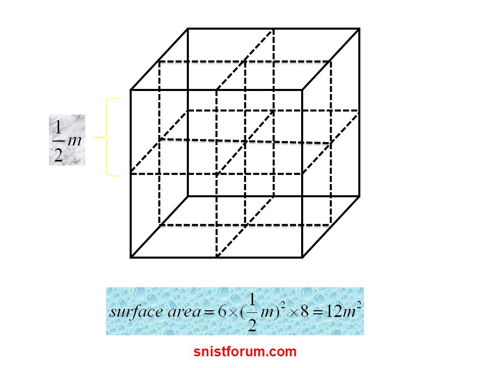
m1

9
Let us consider one Cubic Volume shown in figure its the Surface Area is 6m 2. When it is divided into eight pieces its Surface Area becomes 12m 2, similarly When the same volume is divided into 27 pieces its Surface Area becomes 18m 2. Thus we find that when the given volume is divided into smaller pieces the Surface Area increases. Hence as particle size decreases a greater proportion of atoms are found at the surface compared to those inside. Nano particles have a much greater surface area per given volume compared with larger particles. It makes materials more Chemically reactive. snistforum.com

11
In Nano Crystals, the Electronic energy levels are not continuous as in the bulk but are discrete (finite density of states), because of the confinement of the electronic Wave function to the physical dimensions of the particles. This phenomenon is called Quantum confinement and therefore Nano Crystals are also referred to as quantum dots (QDs). Quantum Confinement snistforum.com
. Quantum Confinement snistforum.com.")
12
Properties of Nano Materials Nano Materials have properties that are different from those of bulk materials. Most Nano structure materials are Crystalline in nature and they posses unique properties. snistforum.com

13
Physical Properties of Nano Particles Crystal structure of Nano particles is same as bulk structure with different lattice parameters. The inter atomic spacing decreases with size and this is due to long range electrostatic forces and the short range core-core repulsion. The Melting point of Nanoparticles decreases with size. snistforum.com

14
Chemical Properties The Electronic structure of Nanoparticles is dependent on its size and the ability of Nano cluster to react, depends on cluster size. The large Surface area to volume ratio the variations in geometry and the electronic structure of Nano particles have a strong effect on catalytic properties. snistforum.com

15
Electrical properties The electronic structure of Nano materials is different from its bulk material. The density of the energy states in the conduction band changes. When the energy spacing between two energy levels is more than K B T, energy gap is created. Nano clusters of different sizes will have different electronic structures and different energy level separations. The Ionization potential at Nano sizes are higher than that for the bulk materials snistforum.com

16
Magnetic Properties The Magnetic Moment of Nano particles is found to be very less when compared them with its bulk size. Nanoparticles made of semiconducting materials Germanium, Silicon and Cadmium are not Semiconductors. snistforum.com

17
Applications of Nanomaterials Chemical Industry: Fillers for point systems Coating Systems based on Nano composites. Magnetic fluids. Automotive Industry: Light weight construction Painting Catalysts Sensors snistforum.com

18
Medicine Drug delivery systems Active agents Medical rapid tests Antimicrobial agents and coatings. Agents in cancer therapy. Electronic Industry Data memory Displays Laser diodes Glass fibers Filters Conductive, antistatic coatings. snistforum.com

19
Energy Sources Fuel cells Solar cells Batteries capacitors. Cosmetics Sun protection creams Tooth paste snistforum.com

20
Production of Nanomaterials There are many methods to produce Nanomaterials Plasma Arcing Chemical Vapor Deposition Sol-gel Electro deposition Ball Milling snistforum.com

21
Plasma Arcing Method Plasma is an ionized gas, and to produce plasma potential difference is applied across two electrodes. Plasma arcing device consists of two electrodes The gas yields up its electrons and gets ionized. In this Method an arc passes from one electrode to the other and the generated ionized gas( plasma ) conducts electricity. Positively charged ions pass to the other electrode pick up the electrons and are deposited to form Nano particles as a Nano Surface. Plasma Arcing is used to produce carbon Nanotubes. snistforum.com
 conducts electricity. Positively charged ions pass to the other electrode pick up the electrons and are deposited to form Nano particles as a Nano Surface. Plasma Arcing is used to produce carbon Nanotubes. snistforum.com.")
22
Chemical Vapor Deposition( CVD) In this method Nanoparticles are deposited from the gas phase. Material is heated to form a gas and then allowed to deposit on a solid surface, usually under vacuum condition. snistforum.com

23
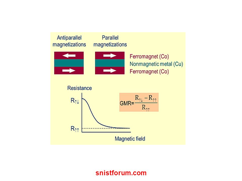
Giant Magneto resistance Like other magneto resistive effects, giant magneto resistance (GMR) is the change in electrical resistance of some materials in response to an applied magnetic field. It was discovered that the application of a magnetic field to magnetic metallic multilayer's such as Fe/Cr and Co/Cu, in which ferromagnetic layers are separated by nonmagnetic spacer layers of a few nm thick, results in a significant reduction of the electrical resistance of the multilayer. This effect was found to be much larger than other magneto resistive effects that had ever been observed in metals and was, therefore, called “giant magneto resistance”. In Fe/Cr and Co/Cu multilayer's the magnitude of GMR can be higher than 100% at low temperatures. snistforum.com

24
The change in the resistance of the multilayer arises when the applied field aligns the magnetic moments of the successive ferromagnetic layers, as is illustrated schematically in the figure below. In the absence of the magnetic field the magnetizations of the ferromagnetic layers are anti parallel. Applying the magnetic field, which aligns the magnetic moments and saturates the magnetization of the multilayer, leads to a drop in the electrical resistance of the multilayer snistforum.com

25
Since discovery in 1988 GMR has generated a lot of interest among academic and industrial laboratories due to deep fundamental physics that controls this phenomenon and tremendous technological potential for magnetic recording, storage and sensor industries. In 2007 Albert Fert and Peter Grünberg were awarded the Nobel Price in Physics for the discovery of GMR snistforum.com

Similar presentations


>")


>")


>")
