Download presentation
Presentation is loading. Please wait.

1
By Satish Chandra Electronics and Communication Engg. SRMCEM,LUCKNOW

2
Usually named as Molecular Electronics. Moletronics is a branch of applied physics which aims at using molecules as passive or active electronic components. These molecules will perform the functions that currently performed by semiconductors.

3
Molecular electronics arose in the late 1950s as a visionary program conducted by Westinghouse on behalf of the Air Force. Molecular electronics reappeared again at IBM in the 1970s and at the Naval Research Laboratory in the 1980s. Researchers from Hewlett-Packard and the University of California, Los Angeles, announced in July 1999 that they’ve actually made logic circuits that use molecular level chemical processes.

5
Optimists. Molecules are small Organic chemistry uses abundant C,N,H,O A mole of molecules/ems would make a hugely dense machine Self assembly will solve the "expensive fab-lines" problem Molecular structures will be inexpensive to make (but defective) FPGA's will provide an approach to configure the machine around defects Molecules can be arranged into the third dimension Pessimists Oxide gates will be 4 atoms thick Inferior electrical properties relative to Cu, AI, Si, and Si02 Performance will be bounded by heat dissipation limitations Show me useful self assembly Making really good devices is less costly than configuring around defects The machine will be all interconnects and possible density gains will thus be lost CMOS is in 2.5 dimensions now ; grain size of poly Si is now bigger than that of a transistor
 FPGA s will provide an approach to configure the machine around defects Molecules can be arranged into the third dimension Pessimists Oxide gates will be 4 atoms thick Inferior electrical properties relative to Cu, AI, Si, and Si02 Performance will be bounded by heat dissipation limitations Show me useful self assembly Making really good devices is less costly than configuring around defects The machine will be all interconnects and possible density gains will thus be lost CMOS is in 2.5 dimensions now ; grain size of poly Si is now bigger than that of a transistor.")
6
Year Transistor Size I If current trend continues, it will reach molecular scale in two decades. T There are many molecules with interesting electronic properties. Semiconductor devices shrink to the nano-scale

7
Fe +3 Fe +2 Heme group e-e- e-e- Au

8
The “bead” can be reversibly switched between two positions by pH.

9
Molecular Motor Molecular Oscillator

12
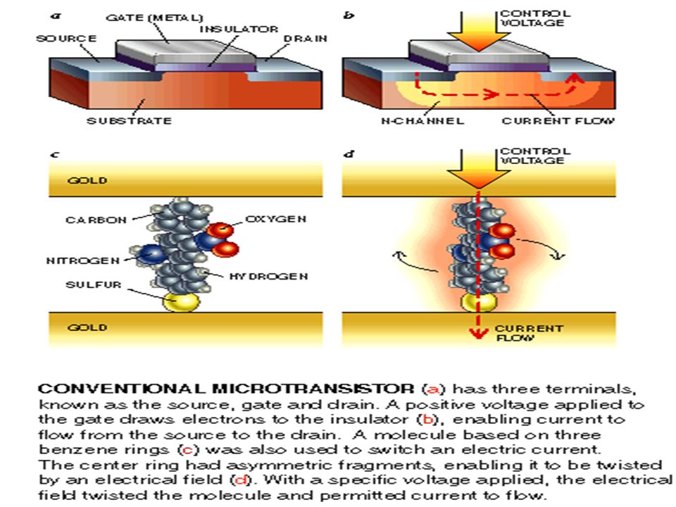
Byphenyl Molecule Diode Behavior at Room Temperature

13
2. For the nitro-amine molecule, we observed strong NDR(negative differential resistance) behavior at low temperature: Nitro-amine Molecule Low Temperature NDR
 behavior at low temperature: Nitro-amine Molecule Low Temperature NDR.")
14
3. The "nitro-only" molecule shows NDR at both low and room temperature: Nitro-only Molecule Low Temperature NDR

17
Molecular Recognition: A capability that Si lacks K + Ag + K + + Crown ether A small difference in the diameters of the K + and Ag + can cause a huge difference in the binding capacity

18
Ultra-dense Molecular Electronic Computer Processor The reliable, hierarchical assembly and fabrication of a prototype molecular electronic computer processor. Local molecular device densities of at least one hundred billion devices per square centimeter or fifty thousand nano devices in a 100 square micron area. Clock rate of at least 10 kilohertz or equivalent. Consuming no more than 10 Watts per square centimeter of power. This nanoprocessor should be programmable and reprogrammable, and it should perform logic functions including arithmetics. Logic and registers should be integrated and in communication with memory. The complexity of the original 1971-vintage microprocessors, i.e. the Intel 4004, but it would be 100,000 times smaller in area. Capable of being integrated with the molecular memory.

19
Capacity to perform 10 12 operation in one second. 10 6 gates operating at 10 6 cycle/sec Largest defect-tolerant computer It has 220,000 hardware defects.

20
Single electron devices. Single atom switching. Switching by biomolecular recognition. Size Power Speed Low Manufacturing Cost Easier to Manufacture

21
Scalability to near molecular dimensions. Tolerance of manufacturing defects. Introduction of non-traditional fabrication methods (e.g. chemically directed self-assembly). Bridging between device densities potentially achievable at molecular scale with those at for standard lithography. Simplicity of fabrication. Key difficulties to be overcome for molecular circuit design
. Bridging between device densities potentially achievable at molecular scale with those at for standard lithography. Simplicity of fabrication. Key difficulties to be overcome for molecular circuit design.")
22
The subject of moletronics has moved from mere conjuncture to an experimental stage. Research in moletronics will naturally dominate the next century. Today is the age of information explosion. Polymer materials hold hopes of rapid development of improved systems and techniques of computing and communications. For e.g., polymer optical fibre has a number of advantages over glass fibres like better ductivity,light weight, higher flexibility is in splicing and insensitivity to stress, etc. all these show that polymers will play a vital role in the coming years and ME shall compete with IC technology which is growing in accordance with Moore’s prediction.

Similar presentations


>")
>")


 Roll Number :67 SUBJECT :PHYSICS SUBJECT CODE :2110011 Presentation By: Kartavya Parmar.>")

2011 Presentation Point(www.presentationpoint.yolasite.c om)>")
