Download presentation
Presentation is loading. Please wait.

2
(a)luminescence (LED) (b)optical amplifiers (c)laser diodes
luminescence (LED) (b)optical amplifiers (c)laser diodes")
3
Electroluminescence devices Light-emitting diode (LED) Semiconductor optical amplifier (SOA) Laser diode (LD) Forward biasing injects into the junction an high number of carrier so that the allowed photon rate increases and become “visible” Emission is not directional
 Semiconductor optical amplifier (SOA) Laser diode (LD) Forward biasing injects into the junction an high number of carrier so that the allowed photon rate increases and become visible Emission is not directional")
4
The necessary balance between the injection rate and the recombination decay (total, radiative or not) gives the density of available excess carriers (pairs/cm 3 ) The total photon flux is the overall flux integrated over the whole emission bandwidth!!!! The total photon flux is given by the total number of carriers divided by the radiative recombination rate

5
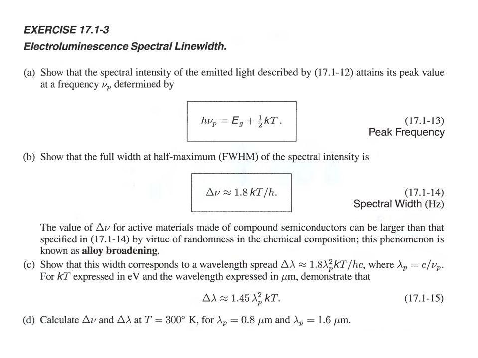
Exercise 17.1-3

7
LED characteristics - + The internal photon flux is directly proportional to the injected current

8
Forward voltage for LEDs

9
Extraction efficiency

10
The total photon flux outside the LED is given by several factors: 1.Absorption in the semiconductor (η 1 =exp(-αl)) 2.Reflection at the surface (η 2 ) 3.Acceptance cone (with no total reflection) In all just a few percent of the created photons come out from the junction Enhancing extraction efficiency The extraction efficiency can be enhanced in a multitude of ways. A spherical dome surrounding a point source at its center permits all rays to escape. hemispherical domes, cylindrical structures (which have an escape ring along the perimeter in addition to the escape cone toward the top surface), inverted cones, and truncated inverted pyramids. However, geometries that entail complex processing steps are often avoided in practice because of increased manufacturing costs.
, inverted cones, and truncated inverted pyramids. However, geometries that entail complex processing steps are often avoided in practice because of increased manufacturing costs..")
11
Extraction efficiency

12
Spatial pattern of emitted light

13
LED characteristics Power-conversion efficiency (or, wall-plug efficiency) Internal efficiency Extraction efficiency External efficiency Luminous efficiency (lm/W)
 Internal efficiency Extraction efficiency External efficiency Luminous efficiency (lm/W)")
15
Pumping may be achieved by the use of external light provided that its photon energy is > E g. Pump photons, absorbed by the semiconductor, generate carrier pairs. The generated electrons and holes decay to the bottom of the conduction band and the top of the valence band, respectively. If the intraband relaxation time is much shorter than the interband relaxation time, as is usually the case, population inversion between the bands is achieved. Charge carriers travel perpendicularly to the p-n junction, whereas photons travel in the plane of the junction.

16
Optical Amplifier parameters Gain Coefficient Gain bandwidth The effective gain depends on the pumping level. The concentration of carrier has a critical value (like a laser threshold) due to the so call transparency point. A point where the gain due to stimulated emission equals the loss so that for an incoming photon one has an output photon. Below the junction absorb radiation, above it amplifies. In the approximation where the thermal contribution to the Fermi functions gives that f g (v) assumes values ±1 in the two cases. The quantity fg (v) depends on both the Fermi function for the conduction band and for the valence band
 due to the so call transparency point. A point where the gain due to stimulated emission equals the loss so that for an incoming photon one has an output photon. Below the junction absorb radiation, above it amplifies. In the approximation where the thermal contribution to the Fermi functions gives that f g (v) assumes values ±1 in the two cases. The quantity fg (v) depends on both the Fermi function for the conduction band and for the valence band.")
17
Optical Amplifier parameters Peak gain Transparency current density The transparency current density depends on l the length (or the thickness) of the diffusion of the minority carriers into the junction. A wider “junction” require an higher current density to reach the transparency point. To build an efficient amplifier it is useful (and recommended) to design structures able to confine the carriers into a small region. The gain coefficient increases both in its width and in its magnitude as the pump- ing rate R is elevated.
 to design structures able to confine the carriers into a small region. The gain coefficient increases both in its width and in its magnitude as the pump- ing rate R is elevated..")
18
Heterostrctures Injected carrier concentration Narrower active region ( l ) is important (Double) Heterostructures l
 is important (Double) Heterostructures l")
19
In such a double heterostructure one obtains: 1.reduction of the effective thickness (carrier are confined into layer 2) 2.increased gain due to optical confinement thanks to the different index of refraction 3.Reduced loss because layer 1 and 3 band-gaps are optically inactive (forbidden being the energy of the laser photons lower than these band-gaps) These kind of device are called quantum-well
 2.increased gain due to optical confinement thanks to the different index of refraction 3.Reduced loss because layer 1 and 3 band-gaps are optically inactive (forbidden being the energy of the laser photons lower than these band-gaps) These kind of device are called quantum-well")
20
Diode Laser So far we have indicated that a semiconductor junction can act, under certain assumption, as an optical amplifier. What is missed to obtain a laser? We “must” reduce the emission bandwidth (so increasing the coherence and the spectral purity of the emitted radiation) and “clean” the emission pattern to a given spatial mode
 and clean the emission pattern to a given spatial mode.")
Similar presentations


 Low dimensional materials: Quantum wells,>")


 Optics (Ch 12) Resonators (Ch 10) Electromagnetic Optics (Ch 5) Wave Optics (Ch 2 & 3) Ray Optics.>")


