Download presentation
Presentation is loading. Please wait.

2
A semiconductor material cannot be viewed as a collection of non interacting atoms, each with its own individual energy levels. Because of the proximity of the atoms in the crystal lattice, the energy levels belong to the system as a whole. Collections of closely spaced energy levels form energy bands. In the ab sence of external excitation, at T == 0° K, these bands are either fully occupied by electrons or totally unoccupied. The lowest-lying unoccupied energy band is called the conduction band while the highest-lying fully occupied energy band is known as the valence band. These two bands are separated by a forbidden band, with bandgap energy Eg. An external energy source (whether thermal, optical, or electronic) can impart energy to an electron in the valence band, causing it to cross the forbidden band and enter the conduction band. This transition leaves a vacancy (hole) behind in the valence band. In the inverse process, electron-hole recombination, an electron decays from the conduction band to fill an empty state in the valence ba nd (provided that one is accessible), generating a photon and/or phonons in the process.
 can impart energy to an electron in the valence band, causing it to cross the forbidden band and enter the conduction band. This transition leaves a vacancy (hole) behind in the valence band. In the inverse process, electron-hole recombination, an electron decays from the conduction band to fill an empty state in the valence ba nd (provided that one is accessible), generating a photon and/or phonons in the process..")
3
The band structure At T>0 some electrons move from the Valence to the Conduction band each leaving behind an hole. Both the electron hole pair contribute to the material conductivity 1. The absorption of a photon can create an electron-hole pair. 2. The recombination of an electron and a hole can result in the emission of a photon.

4
Si GaAs

5
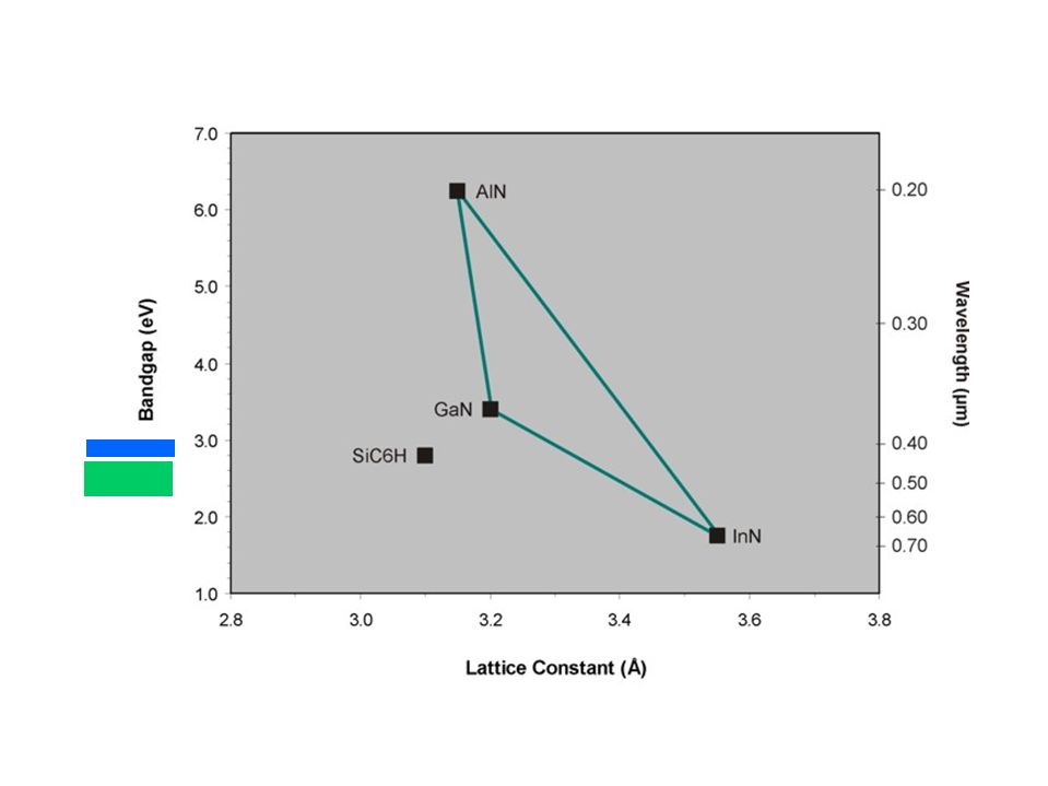
Elemental Semiconductors (IV group) Silicon (Si) and germanium (Ge) Both Si and Ge also find widespread use in photonics, principally as photodetectors. These materials have traditionally not been used for the fabrication of light emitters because of their indirect bandgaps. Binary III-V Semiconductors Compounds formed by combining an elemen t in III, such as aluminum (AI), gallium (Ga), or indium (In), with an element in V, such as nitrogen (N), phosphorus (P), arsenic (As), or antimony (Sb), are important semiconductors. Photon sources (light-emitting diodes and la sers) and detectors can be readily fabricated from many of these binary compounds. They cover a wide range of wavelengths (different bandgaps) The bandgap can be tuned, and so is the optical wavelength, by ternary semiconductors where two elements of III with one element from V (or one from III with two from V) are mixed in a variable ratio.
, gallium (Ga), or indium (In), with an element in V, such as nitrogen (N), phosphorus (P), arsenic (As), or antimony (Sb), are important semiconductors. Photon sources (light-emitting diodes and la sers) and detectors can be readily fabricated from many of these binary compounds. They cover a wide range of wavelengths (different bandgaps) The bandgap can be tuned, and so is the optical wavelength, by ternary semiconductors where two elements of III with one element from V (or one from III with two from V) are mixed in a variable ratio..")
6
Semiconductor materials Selected Elemental and Ill-V Binary Semiconductors Their Bandgap Energies E g, at T = 300 K, Bandgap Wavelengths g = hc /E g, Type of Gap I = Indirect D = Direct Crystal structure D = Diamond Z = Zincblende W = Wurtzite

7
The electrical and optical properties of semiconductors can be modified substantially by the controlled introduction into the material of small amounts of specially chosen impurities called dopants. The introduction of these impurities can alter the concentration of mobile charge carriers by many orders of magnitude. Dopants with excess valence electrons, called donors, replacing a small proportion of the normal atoms, create a predominance of mobile electrons. The material is then said to be an n-type semiconductor. (atoms from column V replacing column-IV atoms in an elemental semiconductor (e.g., Si or Ge), or atoms from column VI replacing column- V atoms in a III-V semiconductor, produce an n-type material. Similarly, a p-type semiconductor is made by using dopants with a deficiency of valence electrons, called acceptors. The result is then a predominance of mobile holes. Column IV atoms in an elemental semiconductor replaced with column-III atoms (e.g., B or In), or column-III atoms in a III-V binary semiconductor replaced with column-II atoms (e.g., Zn or Cd), yield p-type material. Column- IV atoms act as donors for column III and as acceptors for column V, and therefore can be used to produce an excess of both electrons and holes in III- V materials. Of course, the charge neutrality of the material is not altered by the introduction of dopants.
, or atoms from column VI replacing column- V atoms in a III-V semiconductor, produce an n-type material. Similarly, a p-type semiconductor is made by using dopants with a deficiency of valence electrons, called acceptors. The result is then a predominance of mobile holes. Column IV atoms in an elemental semiconductor replaced with column-III atoms (e.g., B or In), or column-III atoms in a III-V binary semiconductor replaced with column-II atoms (e.g., Zn or Cd), yield p-type material. Column- IV atoms act as donors for column III and as acceptors for column V, and therefore can be used to produce an excess of both electrons and holes in III- V materials. Of course, the charge neutrality of the material is not altered by the introduction of dopants..")
8
UV Optical fiber communication

10
Electron-Hole generation radiative recombination : photons nonradiative recombination : lattice vibrations (phonons), Auger process The thermal excitation of electrons from the valence band into the conduction band results in the electron-hole generation Electron-Hole recombination A semiconductor in thermal equilibrium with carrier concentrations n o and p o has equal rates of generation and recombination R injection rate
, Auger process The thermal excitation of electrons from the valence band into the conduction band results in the electron-hole generation Electron-Hole recombination A semiconductor in thermal equilibrium with carrier concentrations n o and p o has equal rates of generation and recombination R injection rate")
11
Internal quantum efficiency the ratio of the radiative electron-hole recombination rate to the total (radiative and nonradiative) recombination rate ( r ). Or, in radiative and nonradiative lifetimes GaN 20 ns0.1 ns 0.005 This parameter is important because it determines the efficiency of light generation (and detection) in a semiconductor material.
 in a semiconductor material..")
12
The role of junctions To realize an a p-n junction two different doped areas are brought into contact. The result is a depletion of carrier in the central region (positive ions on the n side, negative ions on the p side). The presence of static charges creates an electrical barrier (the electrical field points from the n to p). Essentially a diode is realised….
. The presence of static charges creates an electrical barrier (the electrical field points from the n to p). Essentially a diode is realised…..")
13
Interaction of photon with semiconductor carriers a)The absorption of a photon creates an electron-hole pair (band-to-band) b)The photon makes one electron to reach an donor (acceptor) doper level c)The electron move upward in the same band (thermalization afterward) (intra-band) a)Band – to – band b)Impurity – to – band c)Free – carrier (intraband) These transitions all contribute to the overall absorption coefficient
The absorption of a photon creates an electron-hole pair (band-to-band) b)The photon makes one electron to reach an donor (acceptor) doper level c)The electron move upward in the same band (thermalization afterward) (intra-band) a)Band – to – band b)Impurity – to – band c)Free – carrier (intraband) These transitions all contribute to the overall absorption coefficient")
14
Absorption coefficient of bulk semiconductors

15
Direct band-to-band absorption and emission can take place only at frequencies for which the photon energy

16
a)absorption b)spontaneous emission c)stimulated emission
absorption b)spontaneous emission c)stimulated emission")
17
Indircet bandgap A phonon must take part in the process!!!!

18
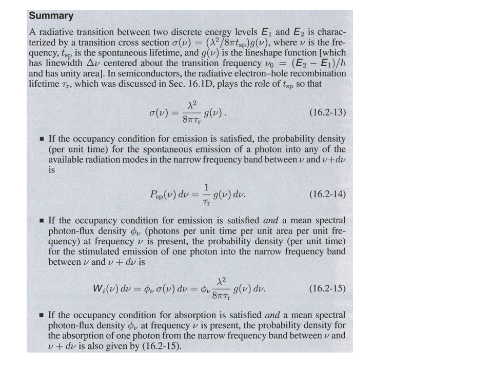
1. The occupancy probabilities depend on the Fermi distribution (and the density of state for the specific semiconductor material…) 2. Then the transition probability depends on the matrix (dipole) element for the given pair of states (initial-final) 3. The availability of states itself is not sufficient for the process to start Each transition has a proper linewidth (much like the atomic linewidth) so that the photon (either absorbed or emitted) has to stay inside the natural lineshape of the transition (there is a multiplicative function)
 2. Then the transition probability depends on the matrix (dipole) element for the given pair of states (initial-final) 3. The availability of states itself is not sufficient for the process to start Each transition has a proper linewidth (much like the atomic linewidth) so that the photon (either absorbed or emitted) has to stay inside the natural lineshape of the transition (there is a multiplicative function).")
20
Spontaneous emission rate and Absorption coefficient Spontaneous Emission Spectral Density in Thermal Equilibrium (direct band-band transition) Absorption Coefficient in Thermal Equilibrium (direct band-band transition) reduced effective mass
 Absorption Coefficient in Thermal Equilibrium (direct band-band transition) reduced effective mass")
21
Refractive index The ability to control the refractive index of a semiconductor is important in the design of many photonic devices, particularly those that make use of optical waveguides, integrated optics, and laser diodes. Semiconductor materials are dispersive, so that the refractive index is dependent on the wavelength.

Similar presentations


>")

 occupied by electrons Not really dealing with isolated atoms, but 3D solids.>")

 silicon – Doping – Carrier concentrations.>")

>")
 Low dimensional materials: Quantum wells,>")


 Also:n 0 p 0 = n.>")


