Download presentation
Presentation is loading. Please wait.

1
RBHD of NOT Gate By: 1. Deep Shah (10BEC089) 2. Divyarajsinh Vaghela (10BEC104)
 2. Divyarajsinh Vaghela (10BEC104)")
2
Outline Purpose Introduction to Radiation Various Radiation Effects Methods to Combat Radiation Effects Why the RHBD Approach? RHBD of NOT Gate References

3
Purpose High level of ionizing radiation cause electrical defects in the CMOS circuits. Historically, radiation immunity was required only for circuits used in Spacecraft and Military environments. Due to continuous decrease in the size of CMOS technologies, the device reliability has become a major concern. With the shrinking feature size, capacitance also reduces which allows even less charge to flip the voltage levels. Therefore, there is significant interest in development of Radiation Hardened Circuits.

4
Introduction to Radiation Radiation is defined as “the process in which energy is emitted as particles or waves.”

5
Types of Radiation Particle Radiation Protons, Neutrons, Electrons, Alpha Particles They have a point of impact on the circuit. Certain part is affected and that too non-uniformly. Photon Radiation X-Rays, Gamma Rays The whole circuit or part of the circuit is under the effect of the radiation. It has a uniform effect on the part under impact.

6
Sources of Radiation Cosmic Rays Gamma Rays Solar Flares Solar particle events Van Allen radiation belts Nuclear reactors & Nuclear explosions

7
Trapped Particles Protons, Electrons, Heavy Ions Galactic Cosmic Rays (GCRs) Solar Protons & Heavier Ions
 Solar Protons & Heavier Ions")
8
Effects of Radiation Important attribute for impact on electronics is how much energy is deposited as it passes through a semiconductor material. This is known as Linear Energy Transfer or LET (dE/dX).
..")
9
Types of Errors Soft Errors Temporary errors or short-time errors Eg. Single Event Transient (SET) cause soft errors Hard Errors Permanent errors Eg. Single Event Upset (SEU) cause hard errors
 cause soft errors Hard Errors Permanent errors Eg. Single Event Upset (SEU) cause hard errors.")
10
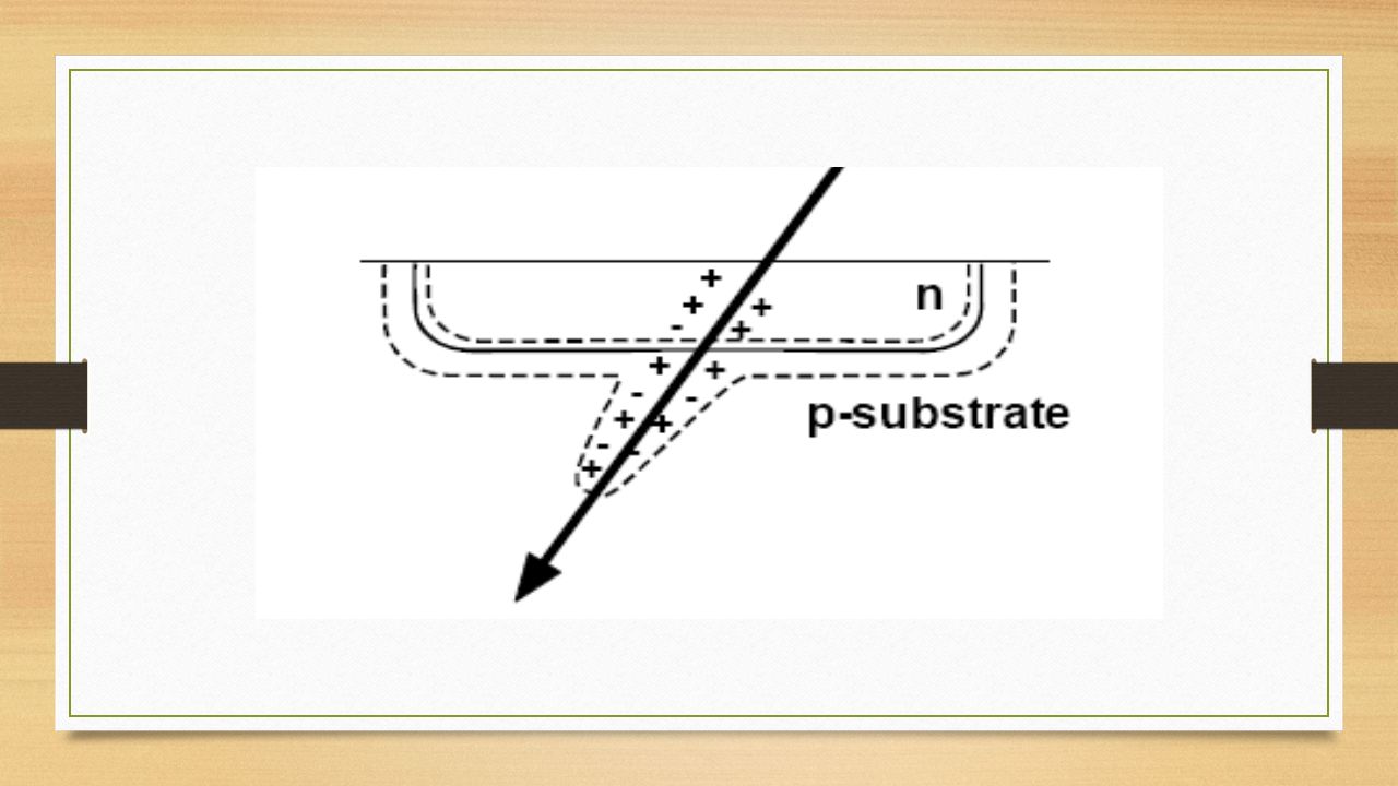
Radiation Effects Displacement Effects: Displacement effects are the manifestations of the displacement of atoms from their normal sites in a crystal lattice to other positions. Total ionizing dose effects: It is the cumulative damage of the semiconductor lattice introduced by ionizing radiation over the exposition time. Charge-Transfer Effects: Energetic radiation can transfer charge within a material and across interfaces as a result of the kinetic energy transferred to secondary particles.

12
Single-Event Effects (SEEs) Single-Event Upset (SEU): They are state changes of memory or register bits caused by a single ion interacting with the chip. In some very sensitive devices, a single ion may introduce a Multiple-Bit Upset (MBU) in several adjacent memory cells. Single-Event Transient (SET): It occurs when the charge collected from an ionization event discharges in the form of a spurious signal traveling through the circuit. In fact, this is the effect of an electrostatic discharge.
 in several adjacent memory cells. Single-Event Transient (SET): It occurs when the charge collected from an ionization event discharges in the form of a spurious signal traveling through the circuit. In fact, this is the effect of an electrostatic discharge..")
14
Circuit Effects Transistor Effects Threshold Voltage Shifts Channel and Junction Leakage Current IC Effects Speed Functional Failure

15
Methods to Combat Radiation Effects

16
1. RHBP RHBP stands for Radiation Hardening By Process Process hardening is proving to be the most effective method of minimizing certain single event effects. However, the technologies that utilize these methods are still large, power hungry, and slow compared to the current industry standards for circuit design. Also these method involves changing the way in which the transistors are fabricated. Hence, it is costly. Eg. Heterojunction Bipolar Transistor (HBT)
.")
17
Standard pixel after irradiation Radiation tolerant pixel after irradiation Enclosed Layout Transistor Thin oxide breaks the leakage current paths

18
RHBD RHBD stands for Radiation Hardening By Design It involves designing the circuit in such a way that it can combat the radiation effects. These can only be done by using more number of transistors, redundancy, more area and consuming more power than the unhardened circuit. But still, for systems where failure is not an option, such circuits in spite of being bulky and slow, prove to be reliable.

19
Various RHBD Techniques Triple Modular Redundancy (TMR) Temporal Hardening Dual Interlock Storage Cells (DICE)
 Temporal Hardening Dual Interlock Storage Cells (DICE)")
20
TMR (Majority Voter)
")
21
Description Triple modular redundant, or TMR, latches and flip-flops mitigate SETs and SEUs through employing spatial hardening by creating multiple critical nodes and physically separating them via layout. This requires the desired circuitry to be placed in triplicate and the sequential logic outputs to be voted on by circuitry such as a majority voter. In this system, if an ion strike effect one of the three circuits, the proper values from the other two circuits will remove the incorrect logic level through the use of a majority voter.

22
TMR (Majority Voter) Advantages It can mitigate both SETs and SEUs. It is robust and reliable than the actual circuit against radiation. Disadvantages Requires 3 times the actual number of required transistors. More area and more power consumption. Requires an extra majority voter circuit.

23
Temporal Hardening

24
Description Instead of physically separating critical nodes and creating multiple circuits, as done in TMR, this technique creates temporal redundancy by separating nodes through the use of delay elements. Delay elements provide a tδ propagation delay from the input, A, to the output, Y. The tδ value is chosen to exceed the maximum SET duration that the circuit is expected to encounter. This insures that any pulse shorter than tδ seen by the nodes Mb, MDb, and MDDb will not reach the majority voter inputs at the same moment and consequently, the latch will mitigate SETs less than that length.

25
Temporal Hardening Advantages It can mitigate SETs. Temporal redundancy can be used in both dual and triple redundant forms. Disadvantages It cannot mitigate SEUs. Requires delay elements and majority voter circuit. More area and power consumption.

26
DICE

27
Description Local redundancy, or interlocking, utilizes feedback storage nodes to mitigate SEUs. A dual interlock storage cell, or DICE, latch consists of eight interlocked inverters but can be simplified down to eight transistors, four PMOS and four NMOS. The feedback paths in this design insure that single node upsets are quickly corrected.

28
DICE Advantages It has a compact, low power design. It can mitigate SEUs. Disadvantages It cannot mitigate upsets caused by multiple node charge collection. When an SET occurs on the input nodes and spans across a clock edge that closes the latch, it stores incorrect logic value.

29
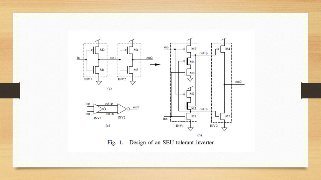
RHBD of NOT Gate

31
Working Assume that both inn and inp are at a logic 0 value. Therefore, out1p and out1n are at logic 1. Now assume that both inn and inp transition to logic 1 due to which transistor M1 turns on and M2 turn off. The turning on of M1 pulls the node out1n down to logic 0 which then turns on M6. Since M6 is ON and M8 is also ON, out1p is driven to a weak logic 02. Both out1p and out1n are now at logic 0, due to which the output of INV2 (out2) goes to logic 1.
 goes to logic 1..")
32
Now when both inputs of INV1 (inn and inp) change to logic 0, then transistor M1 turns off and M2 turns on. As M2 is on, out1p charges to logic 1, which turns M5 on and hence, node out1n is pulled to a weak logic 1 (VDD- V M5 T volts) since M7 is also ON. Since out1n and out1p are both at logic 1, the node out2 is driven to logic 0. Thus, INV1 of Figure behaves like an inverter, with the output node out1p (out1n) switching between VDD and |VT M6 | (VDD - VT M5 and GND). Note that the transistors M5 and M6 of INV1 of Figure 3.1 (b) are selected to be low threshold voltage transistors (indicated by a thicker line in the figure). This is done so as to increase the voltage swing at nodes out1p and out1n, and bring them closer to the rail voltages.
 since M7 is also ON. Since out1n and out1p are both at logic 1, the node out2 is driven to logic 0. Thus, INV1 of Figure behaves like an inverter, with the output node out1p (out1n) switching between VDD and |VT M6 | (VDD - VT M5 and GND). Note that the transistors M5 and M6 of INV1 of Figure 3.1 (b) are selected to be low threshold voltage transistors (indicated by a thicker line in the figure). This is done so as to increase the voltage swing at nodes out1p and out1n, and bring them closer to the rail voltages..")
33
The inverter INV1 of Figure 1 (b) is tolerant to a radiation strike at out1p and out1n. Consider the case when the nodes inp and inn are at VDD, which implies that out1p and out1n are at |VT M6| and GND respectively, and out2 is at the VDD value. Now suppose a radiation particle strikes at node out1p (the radiation particle strikes either M2 or M6) which increases the voltage at node out1p to VDD (due to the positive charge collection at out1p). Due to this, M4 of INV2 turns off and M5 turn on. However, the node out1n remains at GND value because M7 is in cutoff. Therefore M3 also remains off. Thus, the node out2 remains at the VDD value in a high impedance state. Eventually, the charge collected at out1p dissipates through M6 and M8 (since inp and inn are at VDD) which brings the voltage at out1pnode back to |VTM6|. At this point, M4 turns on again. In this way, the radiation strike at out1p does not affect the out2 node voltage value.
 which increases the voltage at node out1p to VDD (due to the positive charge collection at out1p). Due to this, M4 of INV2 turns off and M5 turn on. However, the node out1n remains at GND value because M7 is in cutoff. Therefore M3 also remains off. Thus, the node out2 remains at the VDD value in a high impedance state. Eventually, the charge collected at out1p dissipates through M6 and M8 (since inp and inn are at VDD) which brings the voltage at out1pnode back to |VTM6|. At this point, M4 turns on again. In this way, the radiation strike at out1p does not affect the out2 node voltage value..")
34
Similarly, a particle strike at out1n does not affect the node out2 when inn and inp are at the GND value. A radiation particle at out1p (out1n) node can only result in a positive (negative) glitch since only PMOS (NMOS) transistors are connected to it. Also this positive (negative) glitch at out1p (out1n) does not propagate to out2. This is because the out1p (out1n) node drives only the PMOS (NMOS) transistor of INV2 which goes into cutoff mode when a positive (negative) glitch appears at out1p (out1n) node. A radiation particle strike at M8 can be of any significance only when out1p is at the VDD value (since a radiation particle strike at the NMOS transistor can only result in a negative glitch). However, when out1p is at VDD, M6 is turned off and hence a particle strike at M8 does not affect out1p node voltage.
 node can only result in a positive (negative) glitch since only PMOS (NMOS) transistors are connected to it. Also this positive (negative) glitch at out1p (out1n) does not propagate to out2. This is because the out1p (out1n) node drives only the PMOS (NMOS) transistor of INV2 which goes into cutoff mode when a positive (negative) glitch appears at out1p (out1n) node. A radiation particle strike at M8 can be of any significance only when out1p is at the VDD value (since a radiation particle strike at the NMOS transistor can only result in a negative glitch). However, when out1p is at VDD, M6 is turned off and hence a particle strike at M8 does not affect out1p node voltage..")
35
Similarly, a radiation particle strike at M7 does not affect the voltage of the out1n node. In this way, INV1 of Figure 1 (b) is tolerant to radiation particle strikes since a particle strike at either of its output nodes does not affect the output of its fan_out gates (like out2 of INV2 of Figure 1 (b)).
 is tolerant to radiation particle strikes since a particle strike at either of its output nodes does not affect the output of its fan_out gates (like out2 of INV2 of Figure 1 (b))..")
36
References Kenneth A. LaBel, “Programmable Logic in the Space Radiation Environment ”, Electronics Radiation Characterization Project Manager. Michal Koziel, “Development of radiation hardened pixel sensors for charged particle detection ”, University of Strasbourg. Rajesh Garg and Sunil P. Khatri, “IEEE Paper On Highly SEU Tolerant Digital Circuit Design Approach ”, Department of ECE, Texas A&M University, College Station TX 77843. Bradley Matush, “An Innovative Radiation Hardened By Design Flip-Flop”, Arizona State University. H. Zhenfeng, L. Huanguo, “A Novel Radiation Hardened by Design Latch,” Journal of Semiconductors, vol. 30, no. 3, March, 2009.

37
Thank You

38
About the Authors

39
Deep Shah Student, Department of Electronics & Communication, Institute of Technology, Nirma University. E-mail: deep.shah.61192@gmail.com

40
Divyarajsinh Vaghela Student, Department of Electronics & Communication, Institute of Technology, Nirma University. E-mail: divyarajsinh13vaghela@gmail.com

Similar presentations


 – Soft Errors By: Rajesh Garg Sunil P. Khatri Department of Electrical and Computer Engineering, Texas A&M University, College.>")


 Elements Charu Nagpal Rajesh Garg Sunil P. Khatri Department.>")


 1 ELEC 7770 Advanced VLSI Design Spring 2007 Soft Errors and Fault-Tolerant Design Vishwani.>")

