Download presentation
Presentation is loading. Please wait.

1
NAME: NIDHI PARMAR ENR.NO.:130800111005 GUIDED BY: RICHA TRIPATHI

2
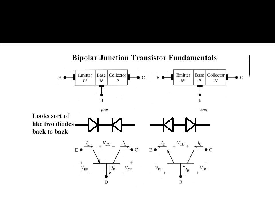
A bipolar transistor is a semi-conductor device that acts as a variable resistor Applications Amplifiers Voltage and Current Regulators Electronic Switches Made up of three alternating layers, which form two P-N junctions. Emitter: heavily doped region that supplies majority current carriers. Base: Thin and lightly doped region that controls current flow through the transistor. Collector: Large, lightly doped region used to collect current carriers from emitter.

3
BJTs – Basic Configurations Fluid Flow Analogy Difference between FET (field effect transistor) and BJT Technology of BJTs pnp BJT npn BJT
 and BJT Technology of BJTs pnp BJT npn BJT")
5
Construction drawing can be simplified as a “sandwich” of semiconductor materials. Can be either NPN or PNP transistor Schematic Symbol: Arrow always points between base and emitter Direction designates type ▪ NPN = Not Pointing iN ▪ PNP = Pointing iN Properly Also points in direction of conventional current flow Collector Base Emitter Collector Base Emitter

6
Base to Emitter Junction (V BE ) Forward biased for majority current carriers to flow from emitter to base, where they become minority carriers Base to Collector Junction (V BC ) Reverse biased to allow minority current carriers from the emitter flow from base to collector Q1Q1 Base Emitter Collector V BE V BC
 Forward biased for majority current carriers to flow from emitter to base, where they become minority carriers Base to Collector Junction (V BC ) Reverse biased to allow minority current carriers from the emitter flow from base to collector Q1Q1 Base Emitter Collector V BE V BC")
9
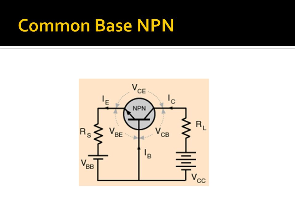
How does I C vary with V CE for various I B ? Note that both dc sources are variable Set V BB to establish a certain I B

10
With the Base to Emitter Junction forward biased, majority current carriers flow from emitter to base, where they become minority carriers This is emitter current (I E ) Since the base is thin and lightly doped, very few current carriers recombine in the base This is base current (I B ) The rest of the current carriers are swept across the base to collector junction This is collector current (I C ) NN P E B C IEIE Conventional Current Flow Electron Current Flow IBIB ICIC
 Since the base is thin and lightly doped, very few current carriers recombine in the base This is base current (I B ) The rest of the current carriers are swept across the base to collector junction This is collector current (I C ) NN P E B C IEIE Conventional Current Flow Electron Current Flow IBIB ICIC")
11
Base to emitter junction is forward biased Low resistance, so small in V BE causes a large in I E The base is thin and lightly doped Few current carriers recombine to form more base current I B only slightly The rest of the current carriers are swept across the base to collector junction I C greatly NN P E B C

12
Current Relationships Emitter current equals base current plus collector current Alpha (α): Ratio of Collector Current to Emitter Current ▪ Typically 0.95 – 0.98 Beta (β): Ratio of Collector Current to Base Current ▪ Ranges from 40 to >100 depending on application Gamma (γ): Ratio of Emitter Current to Base Current ▪ Slightly greater than β
: Ratio of Collector Current to Emitter Current ▪ Typically 0.95 – 0.98 Beta (β): Ratio of Collector Current to Base Current ▪ Ranges from 40 to >100 depending on application Gamma (γ): Ratio of Emitter Current to Base Current ▪ Slightly greater than β")
13
Typical Characteristic Curve Shows relationship between I B, I C and V CE I C relatively constant for a given V CE I C dependant on I B Saturation I C no longer increases for an increase in I B ▪ I C is maximum ▪ V CE is minimum (V CE ≈ 0.2VDC) “ON” state when used as a switch Cutoff Transistor not biased to conduct ▪ I B, I C, I E = 0A ▪ V CE is maximum for circuit “OFF” state when used as a switch Saturation Cutoff
 ON state when used as a switch Cutoff Transistor not biased to conduct ▪ I B, I C, I E = 0A ▪ V CE is maximum for circuit OFF state when used as a switch Saturation Cutoff")
14
Load Line Straight line drawn between saturation and cutoff, representing range of operating points Quiescent Point (Q-Point) The steady-state values of I B, I C, and V CE with no AC input applied Determined by circuit design Saturation Cutoff Q-Point Load Line
 The steady-state values of I B, I C, and V CE with no AC input applied Determined by circuit design Saturation Cutoff Q-Point Load Line")
15
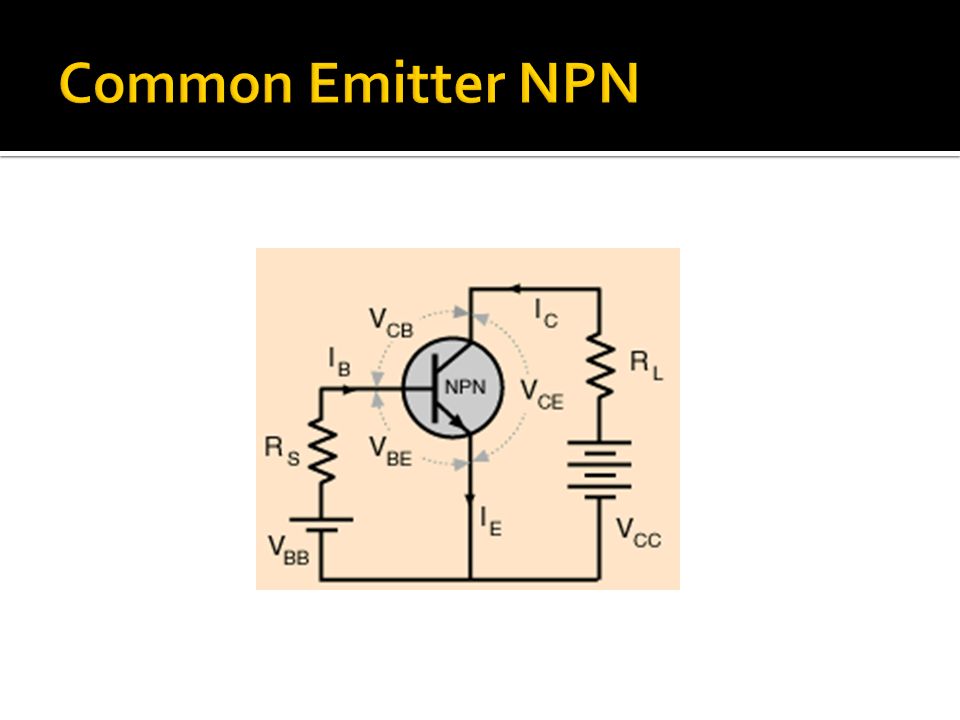
Emitter is “common” to both input and output Input applied to base to change V BE Output taken from collector Gain Medium voltage gain and current gain High power gain Impedance Medium input and output impedance +V CC RBRB RCRC V out V in Q1Q1 C1C1 IBIB ICIC IEIE

16
Positive Half Cycle V in (+) V b (+) V be I b, I c, I e V RC V c (+) V out (+) Negative Half Cycle V in (-) V b (+) V be I b, I c, I e V RC V c (+) V out (+) Output is 180° out of phase with input +V CC RBRB RCRC V out V in Q1Q1 C1C1 IBIB ICIC IEIE
 V b (+) V be I b, I c, I e V RC V c (+) V out (+) Negative Half Cycle V in (-) V b (+) V be I b, I c, I e V RC V c (+) V out (+) Output is 180° out of phase with input +V CC RBRB RCRC V out V in Q1Q1 C1C1 IBIB ICIC IEIE")
17
Positive Half Cycle V in (+) V b (+) V be I b, I c, I e V RC V c (+) V out (+) Negative Half Cycle V in (-) V b (+) V be I b, I c, I e V RC V c (+) V out (+) Output is 180° out of phase with input V C / V out VBVB V in t t V E / GND
 V b (+) V be I b, I c, I e V RC V c (+) V out (+) Negative Half Cycle V in (-) V b (+) V be I b, I c, I e V RC V c (+) V out (+) Output is 180° out of phase with input V C / V out VBVB V in t t V E / GND")
Similar presentations


 NPNPNP.>")

>")


 –pnp (less common) N P N e b c P N P e b c.>")


 –3 layers of doped semiconductor –2 p-n junctions –Layers.>")
