Download presentation
Presentation is loading. Please wait.

1
LECTURE 5 BASICS OF SEMICONDUCTOR PHYSICS

2
SEMICONDUCTOR MATERIALS

8
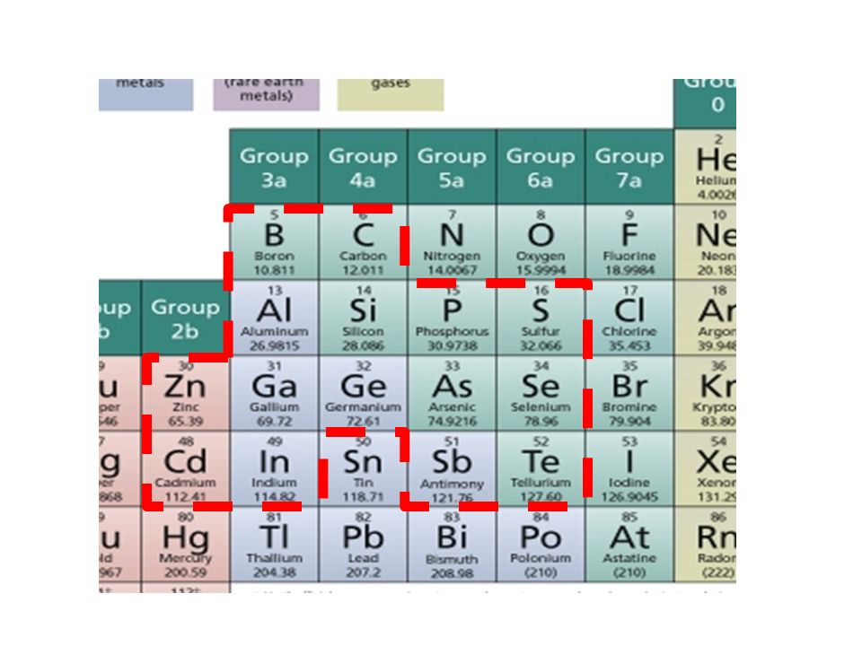
ELEMENTAL IV COMPOUND BINARY III-V BINARY II-VI Si SiC AlP ZnS Ge SiGe AlAs ZnSe AlSb ZnTe GaP CdS GaAs CdSe GaSb CdTe InP InAs InSb Wide variety of electronic and optical properties making the semiconductor as the most favored materials in the design and fabrication of electronics and optoelectronics products

9
Si is used in standard CMOS fabrication GaAs and SiGe are commonly used in high speed devices GaAs and GaP commonly used in LED ZnS (II-VI) television screen InSb, CdSe, PbTe, HgCdTe as light detectors InP for microwave devices GaAs, AlGaAs as semiconductor lasers
 television screen InSb, CdSe, PbTe, HgCdTe as light detectors InP for microwave devices GaAs, AlGaAs as semiconductor lasers")
11
CRYSTAL PROPERTIES OF SEMICONDUCTORS

12
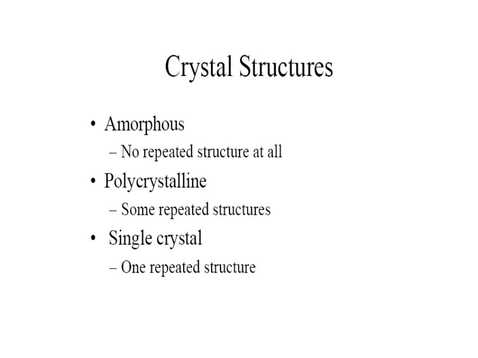
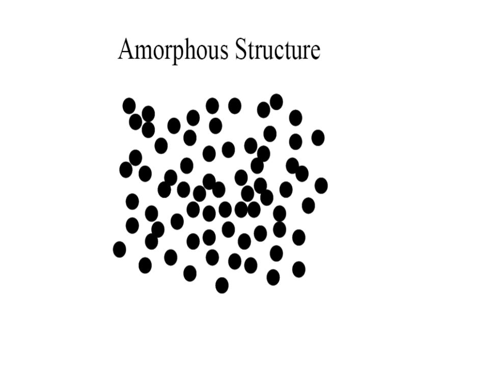
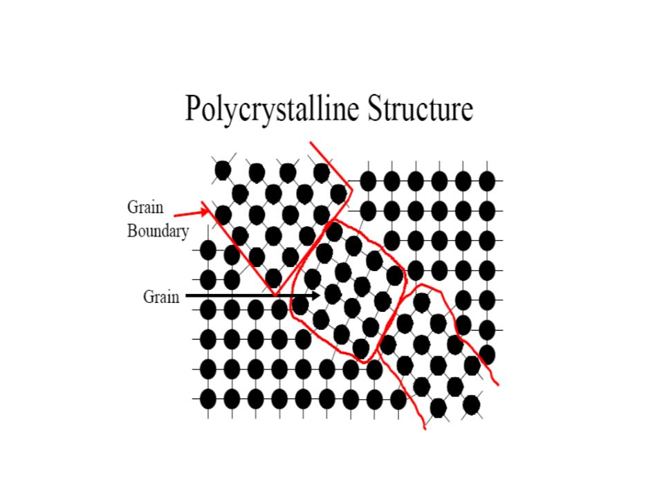
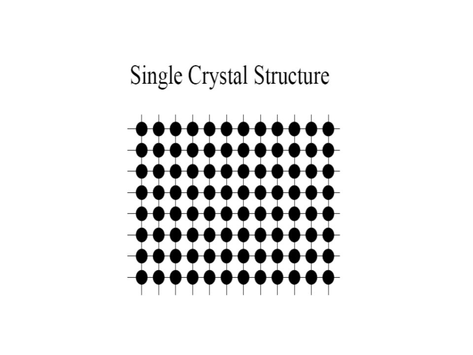
SOLIDS CAN BE CLASSIFIED INTO 3 CATEGORY BASED ON THE ATOMIC ARRANGEMENT AMORPHOUS POLY CRYSTAL SINGLE CRYSTAL

13
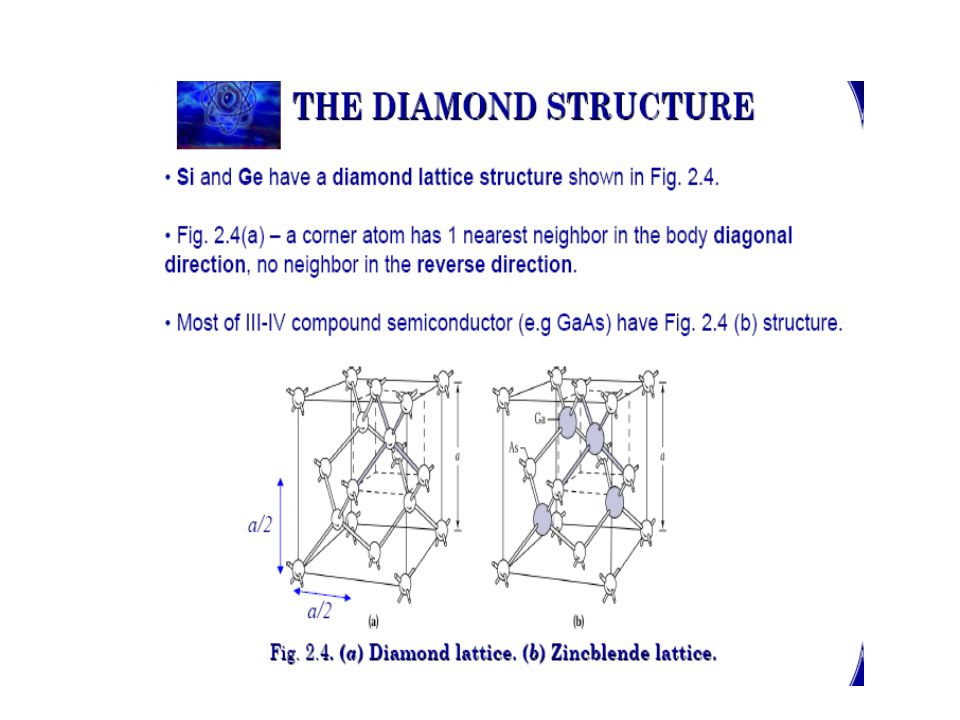
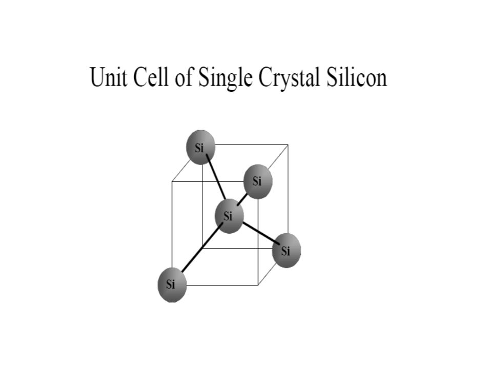
LATTICE LATTICE IS THE PERIODIC ARRANGEMENT OF ATOMS IN A CRYSTAL. UNIT CELL IS THE BASIC BUILDING BLOCK OF CRYSTAL LATTICE. REPEATING ITSELF FOR ENTIRE LATTICE THE SIMPLEST 3D LATTICE IS IN CUBIC FORM (BASIC LATTICE FOR SEMICONDUCTOR MATERIAL IS DIAMOND LATTICE) PROPERTIES OF PERIODIC CRYSTAL LATTICE DETERMINE THE ALLOWED ENERGIES OF ELECTRONS THAT PARTICIPATE IN THE CONDUCTION PROCESS.
 PROPERTIES OF PERIODIC CRYSTAL LATTICE DETERMINE THE ALLOWED ENERGIES OF ELECTRONS THAT PARTICIPATE IN THE CONDUCTION PROCESS..")
14
SIMPLE CUBIC (P) BODY-CENTERED (Na, W) FACE-CENTERED (Al, Au) SIMPLE CUBIC HAS AN ATOM LOCATED AT EACH CORNER OF UNIT CELL BODY CENTERED CUBIC HAS AN ADDITIONAL ATOM AT THE CENTER OF THE CUBE FACE CENTERED CUBIC HAS ATOMS AT THE EIGHT CORNERS AND CENTERED ON THE SIX FACES.
 BODY-CENTERED (Na, W) FACE-CENTERED (Al, Au) SIMPLE CUBIC HAS AN ATOM LOCATED AT EACH CORNER OF UNIT CELL BODY CENTERED CUBIC HAS AN ADDITIONAL ATOM AT THE CENTER OF THE CUBE FACE CENTERED CUBIC HAS ATOMS AT THE EIGHT CORNERS AND CENTERED ON THE SIX FACES.")
22
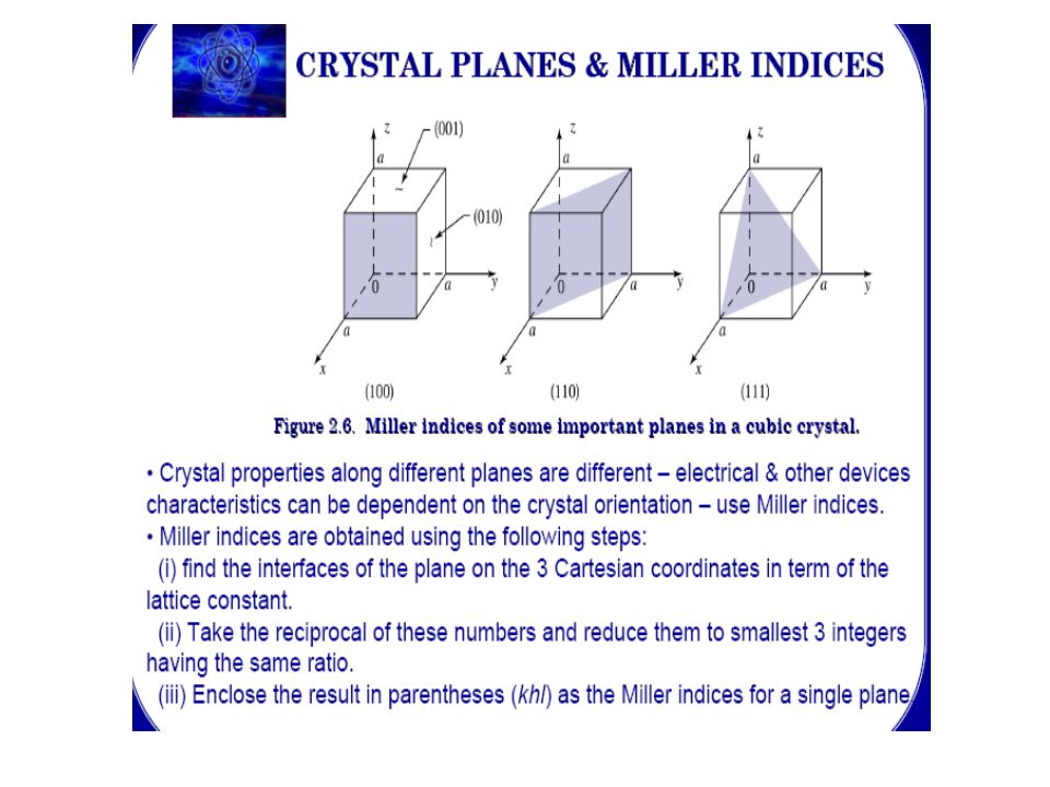
z x y b c a illustrated plane intercepts at 2 a, 4 b and 1 c along 3 crystal axis taking reciprocal, we get ½, ¼, and 1 multiplying each by 4, we get 2, 1 and 4 Thus the plan can be referred as (214) plane – (hkl) h, k and l are called the Miller Indices These numbers define a set of parallel plane in the lattice Example on how to calculate Miller Indices
 plane – (hkl) h, k and l are called the Miller Indices These numbers define a set of parallel plane in the lattice Example on how to calculate Miller Indices")
23
ENERGY BANDS AND CARRIER CONCENTRATION IN THERMAL EQUILIBRIUM

24
QUANTUM MECHANICS CLASSICAL MECHANICS FAILED TO DESCRIBE THE BEHAVIOR OF ELECTRON IN THE MICROSCOPIC SCALE (THE FAILURE OF NEWTON’S LAW OF MOTION TO EXPLAIN THE BAHAVIOR OF ELECTRONS AND HIGH-FREQUENCY ELECTROMAGNETIC WAVES) QUANTUM MECHANICS IS DEVELOPED
 QUANTUM MECHANICS IS DEVELOPED")
25
BASED ON THREE MAIN PRINCIPLES 1.PRINCIPLE OF ENERGY QUANTA 2.WAVE-PARTICLE DUALITY 3.HEISENBERG UNCERTAINTY PRINCIPLE

26
METAL e Light, E = hv PHOTOELECTRIC EFFECT Observations at constant incident intensity, max kinetic energy of emitted electrons varies linearly with the frequency of incident light, v with minimum incident frequency v 0 Based on this experiment, Planck postulated that thermal radiation is emitted from a heated surface in discrete packets of energy called QUANTA. The energy of this quanta is given by, E = hv where h is Planck constant. h = 6.625 x 10 -34 J-s Minimum energy required to remove an electron is called WORK FUNCTION of the material, E = hv o

27
Example Calculate the photon energy of x-ray with the wave-length of λ = 0.708 x 10 -8 cm in the unit of ev? E = h v ; where v = c / λ (6.625 x 10 -34 ) (3 x 10 10 ) = ____________________ = 2.81 x 10 -15 J 0.708 x 10 -8 To convert into unit of ev E = (2.81 x 10 -15 ) / (1.6 x 10 -19 ) = 1.75 x 10 4 ev
 (3 x ) = ____________________ = 2.81 x J x To convert into unit of ev E = (2.81 x ) / (1.6 x ) = 1.75 x 10 4 ev.")
28
SCHRODINGER’S WAVE EQUATION NEW MECHANICS TO EXPLAIN VARIOUS MICROSCOPIC PHENOMENA WAVE MECHANICS, BASED ON PRINCIPS OF ENERGY IN QUANTA AND WAVE-PARTICLE DUALITY. CALLED SCHRODINGER’S WAVE EQUATION 1-D Equation (BASIC POSTULATE OF QUANTUM MECHANICS); -ħ 2. ∂ 2 Ψ (x, t) ___ _________ 2 m ∂ x 2 + V(x) Ψ (x, t) = j ħ ∂ Ψ (x, t) _________ ∂ t Describe behavior of electron movement in a crystal Where Ψ (x, t) is wave function, ħ = h / 2π, V(x) is potential function m is mass of particle, j = √-1 ….. (1)
; -ħ 2. ∂ 2 Ψ (x, t) ___ _________ 2 m ∂ x 2 + V(x) Ψ (x, t) = j ħ ∂ Ψ (x, t) _________ ∂ t Describe behavior of electron movement in a crystal Where Ψ (x, t) is wave function, ħ = h / 2π, V(x) is potential function m is mass of particle, j = √-1 ….. (1).")
29
APPLICATIONS OF SCHRODINGER’S WAVE EQUATION 1.Electron is free space; i.e. no force acting on the particle 2.Particle in Infinite Potential Well (bound particle) V(x) ∞ ∞ X=0 X=a Region I Region II Region III
 V(x) ∞ ∞ X=0 X=a Region I Region II Region III.")
30
The particle is assumed to exist in region II, so it contained within finite region of space. From Equation 1, Total Energy of Particle can be re-write as; ∂ 2 φ (x) _______ ∂x 2 + 2m _____ ħ2ħ2 (E – V(x)) φ (x) = 0 …. (2) If E is finite, the wave function, or φ (x) must be = 0 in region I and III, because this particle cannot penetrate infinite potential barriers. So, the probability of finding the particle in both regions is zero.
 _______ ∂x 2 + 2m _____ ħ2ħ2 (E – V(x)) φ (x) = 0 …. (2) If E is finite, the wave function, or φ (x) must be = 0 in region I and III, because this particle cannot penetrate infinite potential barriers. So, the probability of finding the particle in both regions is zero..")
31
In region II, where V = 0, equation (2) becomes; ∂ 2 φ (x) _______ ∂x 2 + 2mE _____ ħ2ħ2 φ (x) = 0 …. (3) Total particle energy E can be written as; E = E n = ħ 2 n 2 π 2 _________ 2 m a 2 where n = 1,2,3,… …..(4)
 Total particle energy E can be written as; E = E n = ħ 2 n 2 π 2 _________ 2 m a 2 where n = 1,2,3,… …..(4).")
32
The wave function now can be given as; AND after applying a rigorous mathematics and boundary conditions; φ (x) = √ 2 sin K x ___ a ….. (5) Where constant K must have discrete values. IMPLYING that the total energy of particle can only have discrete values. This result means that the energy of particle is quantized !!! (contrary to classical mechanics that allow a continuous energy values for particle).
 Where constant K must have discrete values. IMPLYING that the total energy of particle can only have discrete values. This result means that the energy of particle is quantized !!. (contrary to classical mechanics that allow a continuous energy values for particle)..")
33
EXAMPLE CALCULATE THE FIRST 3 ENERGY LEVELS OF AN ELECTRON IN AN INFINITE POTENTIAL WELL. ASSUME THE WIDTH OF THE WELL IS 5Å. From equation we have E n = ħ 2 n 2 π 2 _________ 2 m a 2 = n 2 (1.054 x 10 -34 ) 2 π 2 __________________ 2 (9.11 x 10 -31 ) (5 x 10 -10 ) 2 = n 2 (2.41 x 10 -19 ) J or E n = ________________ n 2 (2.41 x 10 -19 ) 1.6 x 10 -19 = n 2 (1.51) eV Then E 1 = 1.51eV, E 2 = 6.04eV, E 3 = 13.59eV
 2 π 2 __________________ 2 (9.11 x ) (5 x ) 2 = n 2 (2.41 x ) J or E n = ________________ n 2 (2.41 x ) 1.6 x = n 2 (1.51) eV Then E 1 = 1.51eV, E 2 = 6.04eV, E 3 = 13.59eV.")
34
SUMMARY Quantum mechanics and schrodinger’s wave equation were applied to determine the behavior of single-electron system in the presence of potential function. We found that an electron bound to an atom or within a finite space can only take only a discrete values of energy. WHAT’S NEXT? To expand the concept of discrete allowable single-electron energy to a band of allowable electron energies in semiconductor crystal. To qualitatively derive the concept of allowed and forbidden energy bands. To determine the properties of electron in a crystal lattice

35
FORMATION OF ENERGY BANDS Consider 2 identical atoms When they are separated and not interacting, they have the same energy When they are brought closer; the wave functions of two atom electrons overlap the interaction results the split of energy levels into 2 discrete energy levels. Electron energy n = 1

39
ELECTRICAL CONDUCTION IN SOLIDS Si Valence bond: 2 electrons of opposite spins e-e- Silicon covalent bonding at T = 0K

40
As the temperature increase above 0K, a few valence bond electrons may gain enough thermal energy to break the bond and jump into the conduction band. As temperature increase further, more bonds broken, more electrons jump to the conduction band and more “empty states” created in the valence band. Si e-e- e Valance band Conduction band EgEg + e-e-

41
CONCEPT OF THE HOLE Si e-e- e-e- e + + e-e- + e-e- +

Similar presentations


 Computers –Human based –Tube based –Solid state based Why do we need computers? –Modeling Analytical- great.>")


>")


