Download presentation
Presentation is loading. Please wait.

1
Laser Measurements (as comparison to test beam data) Florian Lütticke University of Bonn 9 th VXD Belle 2 Workshop Valencia, 14.01.2016
 Florian Lütticke University of Bonn 9 th VXD Belle 2 Workshop Valencia,")
2
Outline Measurement Setup Drift/HV Measurements CCG/Clear Measurements Large area scan Large area scan at low HV Transistor characteristics of PXD 9 2luetticke@physik.uni-bonn.de … and sorry for using so much color!

3
Setup luetticke@physik.uni-bonn.de Hybrid 6 optics Laser Reflection of me, taking a picture of the lasersystem Motor table

4
Measurement Setup Measurement: Move laser over the matrix At each point take 800 frames Step width: 5 um in both directions 8*10 pixels from 2 gates Analysis: Create mapping between laser position and firing pixel Using the mapping filter out noise hits Calculate seed signal, cluster signal, cluster size, etc.. for each position Caveat: “high” noise when running at 128ns per gate. Solution: Read each gate twice, throw away first reading luetticke@physik.uni-bonn.de4 Probably dust

5
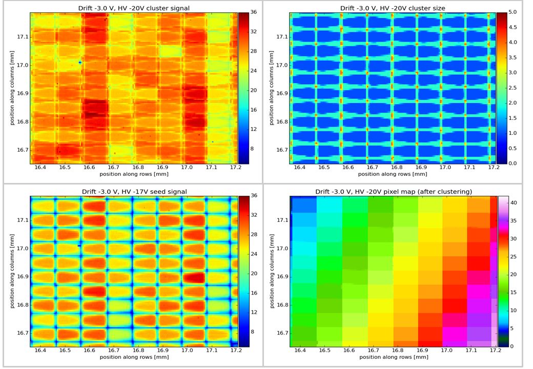
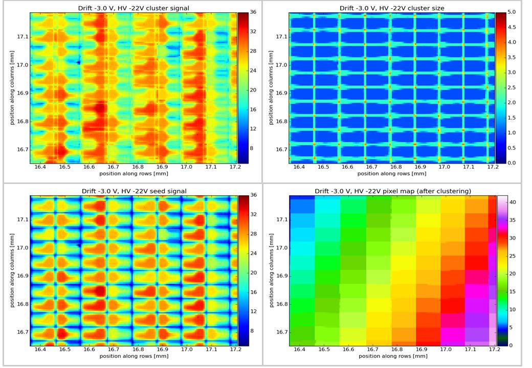
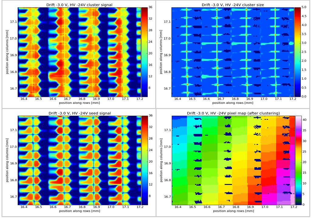
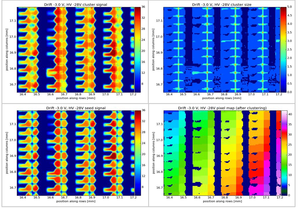
luetticke@physik.uni-bonn.de5 Drift -1VDrift -2V Drift -4V Drift -5VDrift -6V Drift -7V HV -22V HV -20V HV -24V HV -19V HV -18V HV -17V HV -16V

6
luetticke@physik.uni-bonn.de6

7
7

8
8

9
9

10
10

11
luetticke@physik.uni-bonn.de11
12
luetticke@physik.uni-bonn.de12
13
luetticke@physik.uni-bonn.de13
14
luetticke@physik.uni-bonn.de14

15
luetticke@physik.uni-bonn.de15
16
luetticke@physik.uni-bonn.de16
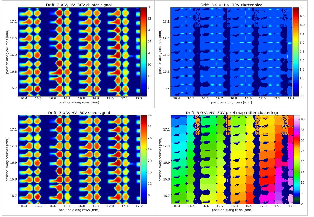
17
luetticke@physik.uni-bonn.de17 HV too negative: –Charge travels close below drift contact and gets into CCG, (like Rainer said). –Near the internal gate, this is not a big effect. –If HV very negative, charge seems to be lost between the pixels (below source and below clear contact)
.")
18
CCG vs Clear voltage Scan luetticke@physik.uni-bonn.de18 First scan: Pedestals –Find a good range to scan What can go wrong? Clear too negative: –Back Emission –Electrons overcome the barrier between clear and internal gate. Electrons from clear contact flood the internal gate. –Can be mitigated by more negative Clear gate. Clear too positive –Clear is attractive for electrons during charge collection –Charge loss

19
CCG vs Clear voltage Scan luetticke@physik.uni-bonn.de19 CCG too negative: –Charge is not able to overcome the CCG Barrier between drift region and internal gate. Stays there long and diffuses -> bigger Clusters in Drift region. –Can be mitigated by high clear –Also: CCG can form a channel between source and drain – high drain currents! –Later effect can be mitigated by positive Clear CCG too positive –Separation between internal gate and clear does not work anymore – Charge loss

20
Clear Gate -1VClear Gate -2V Clear Gate -3V Clearlow 5V Clearlow 4V Clearlow 3V Cluster Signal

21
Clear Gate -1VClear Gate -2V Clear Gate -3V Clearlow 5V Clearlow 4V Clearlow 3V Seed Pixel position

22
Clear Gate -1VClear Gate -2V Clear Gate -3V Clearlow 5V Clearlow 4V Clearlow 3V Cluster size

23
Large Laserscan Scan most of the matrix with the laser On each step: move module, trigger system, check data integrity –Roughly I get 2000 laser points per hour (1.6 sec per point) –5 um step size not doable on 153.000.000 um^2 (6 Million points, 4-5 months) Each ~6000 steps take pedestals Step size 11um and 22um (Pixel size is 50um x 100 um) –4-5 steps per pixel –Step size does not divide pixel size – can be used to project scans of multiple pixels onto a standard pixel and get better resoultion –Small enough to guarantee to have a laser spot in the center of pixel (gain determination) –Still takes rather long (around two weeks, perfect for ) luetticke@physik.uni-bonn.de23
 –5 um step size not doable on um^2 (6 Million points, 4-5 months) Each ~6000 steps take pedestals Step size 11um and 22um (Pixel size is 50um x 100 um) –4-5 steps per pixel –Step size does not divide pixel size – can be used to project scans of multiple pixels onto a standard pixel and get better resoultion –Small enough to guarantee to have a laser spot in the center of pixel (gain determination) –Still takes rather long (around two weeks, perfect for )")
24
Uncorrected pedestals luetticke@physik.uni-bonn.de24 Very low pedestal currents (way outside of dynamic range) Col Row
 Col Row")
25
Corrected pedestals luetticke@physik.uni-bonn.de25 Very low pedestal currents (way outside of dynamic range) Area scanned by laser Col Row
 Area scanned by laser Col Row")
26
Large Laserscan luetticke@physik.uni-bonn.de26 Col Row

27
Large Laserscan luetticke@physik.uni-bonn.de27

28
Large Laserscan luetticke@physik.uni-bonn.de28

29
Large Laserscan luetticke@physik.uni-bonn.de29

30
Large Laserscan @ HV=-14V luetticke@physik.uni-bonn.de30 Col Row

31
Large Laserscan @ HV=-14V luetticke@physik.uni-bonn.de31 Col Row

32
PXD 9 TRANSISTOR CHARACTERISTICS luetticke@physik.uni-bonn.de32

33
PXD9: Measurement of DEPFET IV curves luetticke@physik.uni-bonn.de33 Task: Change V GS, measure I DS Use ADC in DCDBp for current measurement ADC has limited range: –Measure I DS vs V GS –Increase I Sub_In –Repeat Assume same V GS, same I DS –Reconstruct I Sub_In –Add I Sub_In to reduce all parts to one curve

34
Summary Optimal voltages of large PXD6 Matrix were determined using Laser scans. –Obvious non ideal operation points were also studied. –Module working very nice (though with lower speed) –Comparison to test beam results will be done soon Large Area scan revealed gain gradient following the pedestal distribution –Expected, due to extreme pedestal distribution –Offset compensation works very nice At low voltages, stripes (rings?) are observed, similar to PXD9 –HV between -15V and -20V work luetticke@physik.uni-bonn.de34
 –Comparison to test beam results will be done soon Large Area scan revealed gain gradient following the pedestal distribution –Expected, due to extreme pedestal distribution –Offset compensation works very nice At low voltages, stripes (rings ) are observed, similar to PXD9 –HV between -15V and -20V work")
Similar presentations
 Atsuhiko Ochi, Yuki Edo (Kobe University) 11 / 12 / 2012 Micromegas weekly meeting 1.>")


 Nov-21 GLDCAL Japan-Korea meeting.>")


