Download presentation
Presentation is loading. Please wait.

1
Quantum Efficiency Improvement of Polarized Electron Source using Strain compensated Superlattice photocathode N. Yamamoto 1, X.G. Jin 1, T. Miyauchi 3, A. Mano 2, M. Hosaka 2, Y. Takashima 2, M. Yamamoto 1 and Y. Takeda 4,3 1. High Energy Accelerator Research Organization (KEK), 2.Synchrotron Radiation Research Center, Nagoya University, 3. Graduate School of Engineering, Nagoya University, 4.Aichi Science & Technology Foundation, Aichi, Japan. International Particle Accelerator Conference 2015 WEAD3 (14:40-15:00, May. 6, 2015)
, 2.Synchrotron Radiation Research Center, Nagoya University, 3. Graduate School of Engineering, Nagoya University, 4.Aichi Science & Technology Foundation, Aichi, Japan. International Particle Accelerator Conference 2015 WEAD3 (14:40-15:00, May. 6, 2015).")
2
Outline 1.Introduction 2.Problem of Conv. PES PC 3.Strained Compensated PC 4.Exp. Results. 5.Summary PES: Polarized Electron source PC: Photocathode Ref. X.G.Kim, et al., APL (2014) ESP : 92% QE : 1.6% 2/14
 ESP : 92% QE : 1.6% 2/14.")
3
1-1.Polarized Electron Source Essential for future linear colliders (LCs) and electron-ion colliders (EICs) High ESP & high QE (Electron Spin Polarization) (Quantum Efficiency) have to be simultaneously realized. LC (ILC) EIC (eRHIC) Electron Polarization > 80 % Bunch charge 4.8 nC3.5 nC Average Current 63 μA50 mA Life time > 2 weekslong Table. Requirement Parameters for Electron source 3/14
 EIC (eRHIC) Electron Polarization > 80 % Bunch charge 4.8 nC3.5 nC Average Current 63 μA50 mA Life time > 2 weekslong Table. Requirement Parameters for Electron source 3/14.")
4
1-2. Past developments NEA-GaAs type Polarized Electron Source GaAs-GaAs x P (1-x) Strained SL LaserElectron High ESP ( > 90%) & QE( ~ 0.5 %) T. Nakanishi et al., NIM A. 455 (2000) T. Nishitani et al., J. Appl. Phy. 97 (2005) Low Thermal Emittance N. Yamamoto et al., J. Appl. Phy. 102 (2007) 4/14 Heavy dope layer (a few nm)
 Strained SL LaserElectron High ESP ( > 90%) & QE( ~ 0.5 %) T. Nakanishi et al., NIM A. 455 (2000) T. Nishitani et al., J. Appl. Phy. 97 (2005) Low Thermal Emittance N. Yamamoto et al., J. Appl. Phy. 102 (2007) 4/14 Heavy dope layer (a few nm).")
5
1-2. Past developments NEA-GaAs type Polarized Electron Source GaAs-GaAs x P (1-x) Strained SL Transmission type photocathode Laser Electron High ESP ( > 90%) & QE( ~ 0.5 %) T. Nakanishi et al., NIM A. 455 (2000) T. Nishitani et al., J. Appl. Phy. 97 (2005) Low Thermal Emittance N. Yamamoto et al., J. Appl. Phy. 102 (2007) High Brightness [IPAC2011’s Talk] N. Yamamoto et al., J. Appl. Phy. 103 (2008) X.G. Jin, et al., APEX, 51, 108004 (2012) 4/14
 Strained SL Transmission type photocathode Laser Electron High ESP ( > 90%) & QE( ~ 0.5 %) T. Nakanishi et al., NIM A. 455 (2000) T. Nishitani et al., J. Appl. Phy. 97 (2005) Low Thermal Emittance N. Yamamoto et al., J. Appl. Phy. 102 (2007) High Brightness [IPAC2011’s Talk] N. Yamamoto et al., J. Appl. Phy. 103 (2008) X.G. Jin, et al., APEX, 51, (2012) 4/14.")
6
1-2. Past developments NEA-GaAs type Polarized Electron Source High ESP ( > 90%) & QE( ~ 0.5 %) T. Nakanishi et al., NIM A. 455 (2000) T. Nishitani et al., J. Appl. Phy. 97 (2005) Low Thermal Emittance N. Yamamoto et al., J. Appl. Phy. 102 (2007) High Brightness [IPAC2011’s Talk] N. Yamamoto et al., J. Appl. Phy. 103 (2008) X.G. Jin, et al., APEX, 51, 108004 (2012) ↓ High ESP ( 92%) & High QE (1.6%) [This talk] X.G.Kim, et al., APL (2014) GaAs-GaAs x P (1-x) Strained SL Transmission type photocathode Strain-Compensated SL Laser Electron 4/14
 T. Nishitani et al., J. Appl. Phy. 97 (2005) Low Thermal Emittance N. Yamamoto et al., J. Appl. Phy. 102 (2007) High Brightness [IPAC2011’s Talk] N. Yamamoto et al., J. Appl. Phy. 103 (2008) X.G. Jin, et al., APEX, 51, (2012) ↓ High ESP ( 92%) & High QE (1.6%) [This talk] X.G.Kim, et al., APL (2014) GaAs-GaAs x P (1-x) Strained SL Transmission type photocathode Strain-Compensated SL Laser Electron 4/14.")
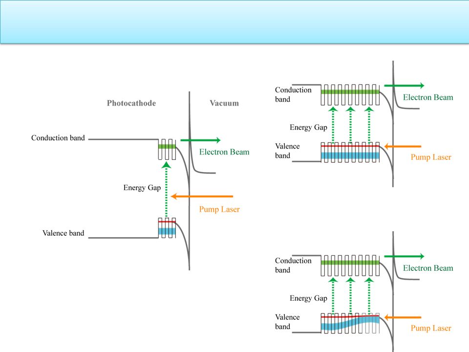
7
1-3. Generation of polarized electron 3 step model 1.Optical pump 2.Diffusion at conduction band 3.Emission from NEA surface 3 step model for electron emission 1.At the SL layers, electrons are pumped by Circularly polarized laser from the valence band to the conduction band. 2. Excited electrons are diffused to PC surface. 3. Electrons are emitted through the NEA surface. 1.At the SL layers, electrons are pumped by Circularly polarized laser from the valence band to the conduction band. 2. Excited electrons are diffused to PC surface. 3. Electrons are emitted through the NEA surface. Vacuum 5/14

8
1-3. Generation of polarized electron 3 step model 1.Optical pump 2.Diffusion at conduction band 3.Emission from NEA surface 3 step model for electron emission 1.At the SL layers, electrons are pumped by Circularly polarized laser from the valence band to the conduction band. 2. Excited electrons are diffused to PC surface. 3. Electrons are emitted through the NEA surface. 1.At the SL layers, electrons are pumped by Circularly polarized laser from the valence band to the conduction band. 2. Excited electrons are diffused to PC surface. 3. Electrons are emitted through the NEA surface. Vacuum To obtain high ESP, Large band split between HH & LH bands is required and obtained by introducing Strain & SL structures. By the way, QE is directly affected by Crystal Quality and SL Thickness. To obtain high ESP, Large band split between HH & LH bands is required and obtained by introducing Strain & SL structures. By the way, QE is directly affected by Crystal Quality and SL Thickness. 5/14

9
1-3. Generation of polarized electron 3 step model 1.Optical pump 2.Diffusion at conduction band 3.Emission from NEA surface 3 step model for electron emission 1.At the SL layers, electrons are pumped by Circularly polarized laser from the valence band to the conduction band. 2. Excited electrons are diffused to PC surface. 3. Electrons are emitted through the NEA surface. 1.At the SL layers, electrons are pumped by Circularly polarized laser from the valence band to the conduction band. 2. Excited electrons are diffused to PC surface. 3. Electrons are emitted through the NEA surface. Vacuum To obtain high ESP, Large band split between HH & LH bands is required and obtained by introducing Strain & SL structures. By the way, QE is directly affected by Crystal Quality and SL Thickness. To obtain high ESP, Large band split between HH & LH bands is required and obtained by introducing Strain & SL structures. By the way, QE is directly affected by Crystal Quality and SL Thickness. 5/14 To realize high ESP & high QE, Keeping Strain SL structure & High Crystalline quality at the same time is key. To realize high ESP & high QE, Keeping Strain SL structure & High Crystalline quality at the same time is key.

10
2.Problem of Conv. Strained SL PC Strain & SL are essential for High ESP, but bringing Bad crystal quality. (Low QE) Ref. X.G.Kim, et al., JAP (2010) Strained SL Fig. TEM image of GaAs/GaAsP Strain SL PC Ref. T. Maruyama, et al., APL (2004) 6/14 SL thickness [nm] 40 140 280
 Ref. X.G.Kim, et al., JAP (2010) Strained SL Fig. TEM image of GaAs/GaAsP Strain SL PC Ref. T. Maruyama, et al., APL (2004) 6/14 SL thickness [nm]")
11
7/14 3.Strain–Compensated SL Strained SL

12
7/14 3.Strain–Compensated SL Strain accumulation Low Crystal quality Strain accumulation Low Crystal quality Strained SL

13
7/14 3.Strain–Compensated SL Strain accumulation Low Crystal quality Strain accumulation Low Crystal quality Strained SL Strain-compensated SL Net strain ≅ 0

14
7/14 3.Strain–Compensated SL High Crystal Quality Higher ESP Higher QE (Thickness SL layers ) Strain accumulation Low Crystal quality Strain accumulation Low Crystal quality Strained SL Strain-compensated SL Net strain ≅ 0 No Strain accumulation
 Strain accumulation Low Crystal quality Strain accumulation Low Crystal quality Strained SL Strain-compensated SL Net strain ≅ 0 No Strain accumulation")
15
4.EXPERIMENTAL &RESULT

16
4-1.GaAs-GaAsP Strain compensated SL GaAs-GaAsP Strain–Compensated SL Al 0.1 Ga 0.9 As 0.81 P 0.19 Buffer Layer : Lattice constant → medium value between GaAs and GaAsP Band gap energy (1.77eV ) → higher than that of SL layers Al 0.1 Ga 0.9 As 0.81 P 0.19 Buffer Layer : Lattice constant → medium value between GaAs and GaAsP Band gap energy (1.77eV ) → higher than that of SL layers Ref. X.G.Kim, et al., APL (2014) 8/14 720 nm
 8/ nm.")
17
4-2.Performances of Strain–Comp. SL SL Thickness Dependence We succeed to fabricate the Strain-Compensated SL PC. ESPs of ~ 90% are obtained below the thickness of 288 nm. QE increases proportionally below the thickness of 500 nm. QEs are improved by using Atomic Hydrogen Cleaning. Q.E. Heat Cleaning Q.E. Atomic Hydrogen Cleaning Limit of Conv. PC (Strained SL) 9/14 * The polarization was measured with back-side laser illumination.
 9/14 * The polarization was measured with back-side laser illumination..")
18
4-2.Performances of Strain–Comp. SL Best Data (Tentative, 24-pair (192 nm) PC) Ref. X.G.Kim, et al., APL (2014) ESP : 92%, QE : 1.6% 10/14
 ESP : 92%, QE : 1.6% 10/14.")
19
4-3. Analysis of Crystal Quality from ESP-QE Spectra Cond. Band Min. LH Band (Valence) HH Band (Valence) Band Gap Mini Band Split Width 11/14 Spin-resolved QE Analysis Band Split Band gap Band Width (HH) Band Width (LH) Energy
 HH Band (Valence) Band Gap Mini Band Split Width 11/14 Spin-resolved QE Analysis Band Split Band gap Band Width (HH) Band Width (LH) Energy.")
20
4-3. Analysis of Crystal Quality from ESP-QE Spectra Design Cond. Band Min. LH Band (Valence) HH Band (Valence) Band Gap Mini Band Split Width 12/14 Design (HH) Design (LH)
 HH Band (Valence) Band Gap Mini Band Split Width 12/14 Design (HH) Design (LH).")
21
Design 4-3. Analysis of Crystal Quality from ESP-QE Spectra Design Design (HH) Design (LH) Cond. Band Min. LH Band (Valence) HH Band (Valence) Band Gap Mini Band Split Width Increasing SL thickness, Crystalline Quality becomes slightly worse. But, IT is not seriously Increasing SL thickness, Crystalline Quality becomes slightly worse. But, IT is not seriously 12/14
 HH Band (Valence) Band Gap Mini Band Split Width Increasing SL thickness, Crystalline Quality becomes slightly worse. But, IT is not seriously Increasing SL thickness, Crystalline Quality becomes slightly worse. But, IT is not seriously 12/14.")
22
4-4.Discussion of ESP degradation Degradation of Spin polarization *1. Ref. X.G.Kim, et al., APEX (2013) 13/14 *The polarization is measured with back-side laser illumination.
 13/14 *The polarization is measured with back-side laser illumination..")
23
4-4.Discussion of ESP degradation Degradation of Spin polarization Observed degradation is understood by spin relaxation during electron transport process. *1. Ref. X.G.Kim, et al., APEX (2013) Spin relaxation during diffusion process ( time constant : 140 ps * 1 ) Spin relaxation during diffusion process ( time constant : 140 ps * 1 ) 13/14 *The polarization is measured with back-side laser illumination.
 Spin relaxation during diffusion process ( time constant : 140 ps * 1 ) Spin relaxation during diffusion process ( time constant : 140 ps * 1 ) 13/14 *The polarization is measured with back-side laser illumination..")
24
Summary GaAs/GaAsP Strain-compensated SL PCs have been developed and were successfully fabricated. – Up to 90 pairs (720 nm) Thickness PCs were tested. – The QEs increase proportional to the SL thickness. – Strain-compensated SL effectively prevents strain accumulations. No Serious Degradation of Crystalline quality was observed. – For thicker PCs, Spin relaxation effect limits the ESP value. Spin relaxation time : 140 ± 12 ps Up to now, Using the 24-pair (192 nm) PC, ESP of 92 % & QE of 1.6 % were achieved. (3 times higher than conv. PC) In future, optimizing the SL thickness, Further QE Improvements is expected. 14/14
 Thickness PCs were tested. – The QEs increase proportional to the SL thickness. – Strain-compensated SL effectively prevents strain accumulations. No Serious Degradation of Crystalline quality was observed. – For thicker PCs, Spin relaxation effect limits the ESP value. Spin relaxation time : 140 ± 12 ps Up to now, Using the 24-pair (192 nm) PC, ESP of 92 % & QE of 1.6 % were achieved. (3 times higher than conv. PC) In future, optimizing the SL thickness, Further QE Improvements is expected. 14/14.")
25
BACK UP SLIDES

26
3.Strain–Compensated SL High Crystal Quality Higher ESP Higher QE (Thickness SL layers ) Strain-compensated SL Net strain ≅ 0 Strained SL Strain accumulation Low Crystal quality Strain accumulation Low Crystal quality 7/14 No Strain accumulation
 Strain-compensated SL Net strain ≅ 0 Strained SL Strain accumulation Low Crystal quality Strain accumulation Low Crystal quality 7/14 No Strain accumulation")
27
歪み補償超格子データの考察 価電子帯 分離幅 伝導帯 重いホール 軽いホール バンドギャップ スピン偏極度と量子効率のスペクトルから 重いホール、軽いホールの量子効率を分離してみる。 EhEh ElEl EhEh ElEl

28
4-3. Analysis of Crystal Quality from ESP-QE Spectra ParameterDesign Value Cond. Band Min. Band width29 meV Light Hole Band width29 meV Heavy Hole Band width < 1 meV Band Split (HH to LH)75 meV Band Gap (HH to CBM)1.54 eV
75 meV Band Gap (HH to CBM)1.54 eV.")
30
Strained super lattice photocathode Band Structure Energy diagram near surface

Similar presentations
 Physics motivations (ii) Principe.>")


. Jordan University of Science.>")


>")
1 Generation of Polarized Electrons by Filed Emission M. Kuwahara A, T. Nakanishi A, S. Okumi A, M.>")
 1/13.>")
