Download presentation
Presentation is loading. Please wait.

1
College Name : Shree Swami Atmanand Saraswati Institute Of Technology(SSASIT)(076) Year : 2 nd year(3 rd sem) EC-2015 Subject Name : Electronic Devices &Circuits(EDC) (2131006) Topic Name : SPECIAL PURPOSE DIODE Prepared By : Bhadani Reshma D. (140760111002) Guided By : Prof.Foram N. Dharsandiya
 Guided By : Prof.Foram N. Dharsandiya.")
2
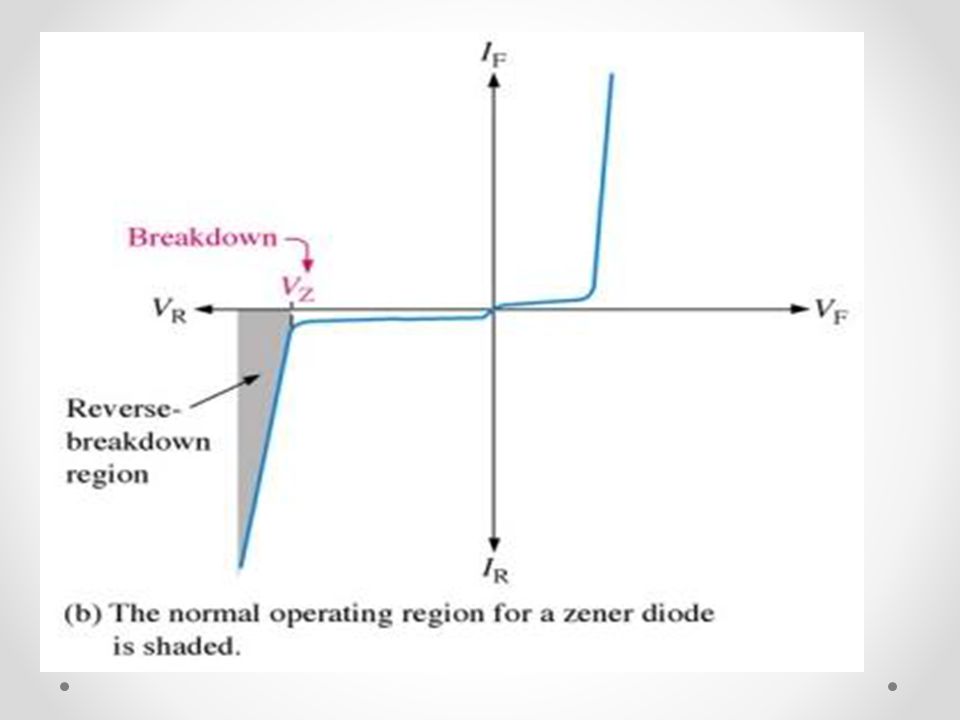
THE ZENER DIODE Zener diodes are commonly used for voltage regulation, that is, they maintain a constant voltage at the output. It is designed to work in the reverse breakdown region. The breakdown voltage is adjusted by controlling the level of doping. The V-I characteristic and zener diode symbol are shown in Figure 1.

3
There are two types of breakdowns in zener diodes. Zener Breakdown Avalanche Breakdown Avalanche breakdown occurs at high voltages typically more than 5 V. Zener breakdown occurs at low voltages typically less than 5 V. Zener Breakdown

5
Breakdown Characteristics As the reverse voltage VR increases from 0V, the reverse current IR remains extremely small. The reverse current starts to increase rapidly when the VR reaches the knee point. The current at this point is called the zener knee current IZK. The breakdown effect starts at this point. After this, the current starts to increase as the zener impedance ZZ decreases. From the knee, the zener voltage VZ remains almost constant.

7
Zener Regulation Keeping the voltage constant across its terminal is the main advantage of zener diode. The minimum zener current required maintaining voltage regulation is IZK. The maximum zener current allowed before it is damaged is IZM. The zener voltage VZ, specified in the datasheets is the voltage at the zener test current IZT.

8
Temperature Coefficient Temperature coefficient () describes the percent change in zener voltage for each degree Celsius change in temperature. The formula for calculating the change in zener voltage Δ is given by Δ=××Δ A positive temperature coefficient means the zener voltage will increase with increase in temperature or decrease with decrease in temperature. A negative temperature coefficient means the zener voltage will decrease with increase in temperature or increase with decrease in temperature.

9
Zener Power Dissipation and Derating Zener diode are specified to operate at the maximum DC power dissipation PD(max). This is given in datasheet of the diode. The power dissipated by a zener diode at any zener current IZ is given as =.

10
ZENER DIODE APPLICATIONS Zener Regulation with a Varying Input Voltage (No Load Condition)
")
11
Zener diode regulators are not veryefficient so they are limited to applications that require low current to the load. Figure 5 illustrates the concept of zener voltage regulation. The zener diode will regulate the output voltage provided > and <<. As the input voltage VIN increases, IZ will increase and there will be very small change in the output voltage +Δ. As the input voltage VIN decreases, IZ will decrease and there will be very small change in the output

12
THE VARACTOR DIODE The junction capacitance of diodes change with reverse bias. Diodes designed to be used as voltage controlled capacitors are called varactors. They always work in reverse bias. The depletion region acts as dielectric and p and n- types act like capacitor plates

13
Basic Operation The capacitance of a material can be determined by plate area A, dielectric constant and plate separation d and is expressed as =/ As the reverse bias increases, the depletion region becomes wide and increases the plate separation d. This decreases the capacitance. As the reverse bias decreases, the depletion region becomes narrow and decreases the plate separation d. This increases the capacitance.

14
OPTICAL DIODES Two types of optical diodes are discussed in this section. Light-Emitting Diode (LED) – These are light emitters. Photodiodes – These are light detectors.
 – These are light emitters. Photodiodes – These are light detectors..")
15
The Light-Emitting Diodes (LED) Basic Operation When the LED is forward biased, electrons cross the pn junction and Recombines with the holes in the p- type. When these high energy electrons recombine with holes, they release energy in the form of photons. The emission of these photons is called electroluminescence.

16
The doping determines the wavelength of the emitted photons.

17
The forward voltage VF across an LED is higher than silicon rectifier diodes (typically between 1.2V to 3.2V). Reverse breakdown is lower than silicon rectifier diodes (3V to 10V). LED Biasing Figure 11(a) shows a typical LED circuit. The graph in Figure 11(b) shows that power of light output is directly proportional to the forward current IF.
. LED Biasing Figure 11(a) shows a typical LED circuit. The graph in Figure 11(b) shows that power of light output is directly proportional to the forward current IF..")
19
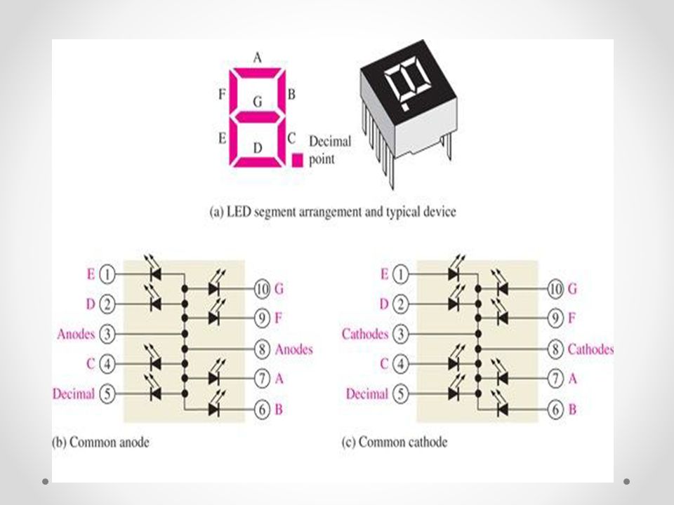
Applications of LED 1. Seven – Segment Display LED’s are widely used in various applications like indicator lights, read out displays etc. A very common application of LED’s is the seven-segment display shown in Figure 12. Each segment is an LED. By forward biasing selected combination of segments, any decimal digits can be formed.

21
2. Remote Controls Infrared LED’s are commonly used in remote controls. Infrared LED emits beam of invisible light. Each button corresponds to an electrical code which is converted to a light code and transmitted through the LED. The receiver recognizes the code and takes the required action.

22
OTHER TYPES OF DIODES There are other types of diodes used for special purpose and applications. They will be discussed in this section. Some of these are The Laser Diode The Schottky Diode The PIN Diode The Tunnel Diode Current Regulator Diode

23
The Laser Diode Laser stands for light amplification by stimulated emission of radiation. Laser light is monochromatic meaning it consists of single light. Construction The pn junction is formed by two layers of doped gallium arsenide. The length of the pn junction is related to the wavelength of the laser.

25
The Schottky Diode Schottky diodes (Figure 21) are high current diodes used in high frequency and fast switching applications. A schottky diode is formed by joining a doped n-type with a metal such as gold, silver of platinum.

26
The forward voltage drop is 0.3V. There are only majority carriers with no reverse leakage current. The metal conductor has many conduction band electrons and n-type is also heavily doped. When forward biased, the n-type electrons move across to the metal region and rapidly loss energy. The process is very fast which makes schottky diodes ideal for fast switching application.

27
The PIN Diode The pin diode consists of heavily doped p and n region separated by intrinsic (i) region In reverse bias, the pin diode acts like a constant capacitance When forward biased, it acts like a current- controlled variable resistance.
 region In reverse bias, the pin diode acts like a constant capacitance When forward biased, it acts like a current- controlled variable resistance.")
28
The Tunnel Diode The tunnel diode exhibit a characteristic known as negative resistance. This makes it useful in oscillator applications. The p and n region of the tunnel diode are heavily doped

29
Current Regulator Diode The current regulator diode keeps a constant current rather than constant voltage as in the case of zener diode. The current regulator works in the forward bias and the forward current remains constant for forward voltage range from 1.5V to 6V. The constant forward current in called the regulator current IP. This device should never be operated in reverse bias.

Similar presentations