Download presentation
Presentation is loading. Please wait.

1
Fermi National Laboratories & Tuskegee University College of Electrical Engineering Aaron Ragsdale: SIST Intern Mentor: Jin-Yuan Wu Summer 2009 SIST Internship

2
Objective Introduction Hardware Firmware Testing Conclusion Acknowledgements References

3
Build an electronic board that utilizes two Field Programmable Gate Arrays(FPGA): Time to Digital Converters(TDC) FPGA- Contains the TDC itself as well at Data Acquisition (DAQ) circuits. Data Acquisition (DAQ) FPGA- interfaces the TDC FPGA, serial port, Ethernet connection, as well as other important components Implement firmware that can be used in many practical applications
 FPGA- interfaces the TDC FPGA, serial port, Ethernet connection, as well as other important components Implement firmware that can be used in many practical applications.")
4
What are Field- Programmable Gate Arrays?(FPGAs) FPGAs are semiconductor devices composed of programmable logic components called “logic blocks” that can be configured and re-configured to perform complex combinational functions.
 FPGAs are semiconductor devices composed of programmable logic components called logic blocks that can be configured and re-configured to perform complex combinational functions.")
5
A Time to digital converter (TDC) is a device that converts signals of pulses into a digital representation of time.
 is a device that converts signals of pulses into a digital representation of time.")
6
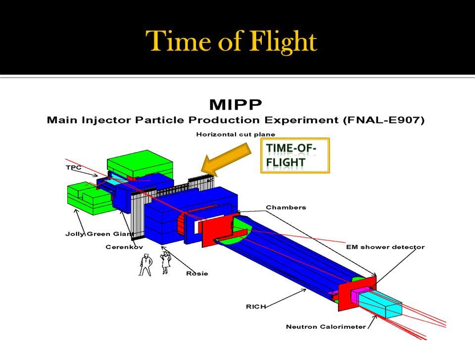
The TDC FPGA has a wide range of applications: High energy Physics Experiments Time-of-Flight (TOF) Fermilab: Main Injector Particle Production Experiment
 Fermilab: Main Injector Particle Production Experiment")
7
MIPP is an experiment studying hadronic flavor particle production at Fermilab. The experiments will cover 1 to 120 GeV/c on multiple targets (liquid Hydrogen, Minos targets and various nuclear targets including Uranium) for six beam species (pion, kaon, protons and their antiparticles). Open geometry spectrometer used to study hadron production. Hadronic fragmentation – test scaling law of particle fragmentation
 for six beam species (pion, kaon, protons and their antiparticles). Open geometry spectrometer used to study hadron production. Hadronic fragmentation – test scaling law of particle fragmentation.")
9
AMP CARDS TDC CARDS

10
Altera Cyclone II FPGA EP25Q208 Altera Cyclone II FPGA EP2C8T144 Ethernet Port : DB9 Converter Serial Port : RJ-45 connector On-Board Signal: Crystal Oscillator (25 MHz) External Signal : BNC Connectors Clock: Crystal Oscillators (50 and 25 MHz) Configuration Chip Serial Connector to USB Blaster
 External Signal : BNC Connectors Clock: Crystal Oscillators (50 and 25 MHz) Configuration Chip Serial Connector to USB Blaster")
11
Ethernet Port Ethernet Chip Configuration Chip Power Supply BNC Connectors TDC FPGA Serial Port DAQ FPGA Crystal Oscillator USB Blaster Connection

12
Firmware: Firmware Schematic-based entry Altera Quartus II Software

13
There were two major problems: The temperature and the voltage power supply were causing uneven bin widths. The wide bins would then limited the time resolution and precision of the TDC.

14
The Cyclone II utilizes a carry chain adder as it delay chain. The registers recodes each bit of the adder result, and a priority encoder follows the array. Questions!? Calibrate: Temperature/Voltage Clock too fast?/ too slow? Synchronizing Input Timing Reference

15
1.Widths of bins are different and varies with supply voltage and temperature. 2.Some bins are ultra-wide due to LAB structure

16
Longer delay line Some signals may be registered twice at two consecutive clock edges. The two measurements can be used: – to calibrate the delay. – to reduce digitization errors.

17
It provides a bin-by-bin calibration at certain temperature. It is a “turn-key” solution. A DNL histogram is booked in the FPGA internal memory. Once all hits are booked into the histogram, the lookup table (LUT) is integrated from the DNL histogram so that it outputs the actual time of the center of the addressed bin.
 is integrated from the DNL histogram so that it outputs the actual time of the center of the addressed bin..")
18
The wave union launcher creates multiple logic transitions after receiving a input logic step Wave Union Launcher In CLK.

19
After arrival of the input, the wave union launcher B starts to oscillate launching a wave union into the carry chain. The carry chain/register array structure takes 16 snap shots of the oscillation bit patterns in 16 clock cycles at 400MHz. The phase of the oscillation is determined by the arrival time of the input signal. Then in the 16 snap shots, the locations of the logic transitions can be utilized to compute the arrival time of the input signal to a higher resolution through the processing block “SumHitD”.

21
Ultra-Wide bins were eliminated

22
Distributing a Timing Reference Once D0 is detected by the decoder the time stamp counter (TS) and event counter (EV) are reset. Each time the D0 marker arrives the least bits of the TS should be 0. Time Stamp

23
Interfaces the TDC FPGA, a Synchronous Dynamic Random Access Memory, the Serial Port, the Ethernet circuit and the VME bus, a flash memory and the USB connection. Element Configuration is essential

24
The firmware was downloaded successfully. The next step was to test it.

25
DAQ Counter as it collects data

26
The TDC FPGA was able to simulate and transmit raw data. A histogram was displayed. Testing

27
The Board functioned well. This TDC FPGA is innovative in that it solved many problems prevalent in the previously developed firmware. Its new flexible firmware enables it to be utilized in many practical applications.

28
Jin-Yuan Wu, my Supervisor Sten Henson SIST Program Committee Dianne Engram Jamieson Olsen Dr. Davenport Kenie Moses

29
[1] A. Amiri, A. Khouas & M. Boukadoum, “On the Timing Uncertainty in Delay-Line-based Time Measurement Applications Targeting FPGAs,” in Circuits and Systems, 2007, IEEE International Symposium on, 7-10 27-30 May 2007 Page(s): 3772 - 3775. [2] J. Song, Q. An & S. Liu, “A high-resolution time-to-digital converter implemented in field-programmable-gate-arrays,” in IEEE Transactions on Nuclear Science, 2005, Pages 236 - 241, vol. 53. [3] M. Lin, G. Tsai, C. Liu, S. Chu, “FPGA-Based High Area Efficient Time-To-Digital IP Design,” in TENCON 2006. 2006 IEEE Region 10 Conference, Nov. 2006 Page(s):1 – 4. [4] J. Wu, Z. Shi & I. Y. Wang, “Firmware-only implementation of time-todigital converter (TDC) in field programmable gate array (FPGA),” in Nuclear Science Symposium Conference Record, 2003 IEEE, 19-25 Oct. 2003 Page(s):177 - 181 Vol. 1.
![[1] A. Amiri, A. Khouas & M.](http://images.slideplayer.com/35/10466814/slides/slide_29.jpg "Boukadoum, On the Timing Uncertainty in Delay-Line-based Time Measurement Applications Targeting FPGAs, in Circuits and Systems, 2007, IEEE International Symposium on, May 2007 Page(s): [2] J. Song, Q. An & S. Liu, A high-resolution time-to-digital converter implemented in field-programmable-gate-arrays, in IEEE Transactions on Nuclear Science, 2005, Pages , vol. 53. [3] M. Lin, G. Tsai, C. Liu, S. Chu, FPGA-Based High Area Efficient Time-To-Digital IP Design, in TENCON IEEE Region 10 Conference, Nov Page(s):1 – 4. [4] J. Wu, Z. Shi & I. Y. Wang, Firmware-only implementation of time-todigital converter (TDC) in field programmable gate array (FPGA), in Nuclear Science Symposium Conference Record, 2003 IEEE, Oct Page(s): Vol. 1..")
Similar presentations

 Lecture 04: Programmable Logic Technology (2/3) Prof. Sherief Reda Division of Engineering, Brown University.>")

 – –a fixed array of AND gates.>")

>")

 logic block diagram; (b) Layout obtained using a Xilinx Virtex 5 FPGA; (c) simplified block diagram of the Virtex 5.>")


 COE 203 Digital Logic Laboratory Dr. Aiman El-Maleh College of Computer Sciences and Engineering.>")
>")


>")
