Download presentation
Presentation is loading. Please wait.

1
EE503 Integrated Circuit Fabrication & Packaging Technology
TOPIC 1 INTRODUCTION TO INTEGRATED CIRCUIT By: Noorfozila Binti Bahari Pensyarah Utama JKE POLISAS

2
TOPICS in EE503 Introduction To Integrated Circuits (IC)
Silicon And Wafer Preparation Integrated Circuit Fabrication Process MOS Transistor Fabrication Integrated Circuit Packaging Technology Integrated Circuit Testing, Yield And Reliability Micro-Electromechanical System (MEMS)
")
3
TOPICS in EE503 Introduction To Integrated Circuits (IC)
IC technology evolution Classification of IC

4
TOPICS in EE503 Silicon And Wafer Preparation

5
TOPICS in EE503 Integrated Circuit Fabrication Process

6
TOPICS in EE503 MOS Transistor Fabrication NMOS transistor
PMOS transistor

7
TOPICS in EE503 Integrated Circuit Packaging Technology

8
TOPICS in EE503 Integrated Circuit Testing, Yield And Reliability
IC testing Defects and Yield Analysis Reliability and Degradation

9
TOPICS in EE503 Micro-Electromechanical System (MEMS)
")
10
Learning Outcomes Understand Integrated Circuit (IC) Technology
At the end of this session, students should be able to: Understand Integrated Circuit (IC) Technology Know the classification of IC
 Technology. Know the classification of IC.")
11
INTRODUCTION TO IC Definition of Integrated circuit
A complex set of tiny components and their interconnections that are imprinted onto a tiny slice of semiconductor material (e.g silicon). Integrated circuits are usually called ICs or chips.
. Integrated circuits are usually called ICs or chips.")
12
History of Semiconductor Industry

13
History of Semiconductor Industry

14
History of Semiconductor Industry

15
Main Applications of IC
Most electronic equipment today use integrated circuit, for example: Computer / Server / workstation TV / Radio / Video Cell Phones Digital Clock Robotic Systems Telecommunication System Automotive Medical Equipment Aerospace Children's Toys Military Field Missile System etc.

16
Advantages of IC i. Small ii. Low Cost iii. Light Weight
iv. Low power consumption v. Easy replacement vi. High reliability - the ability of a system or component to perform its required functions under stated conditions for a specified period of time.

17
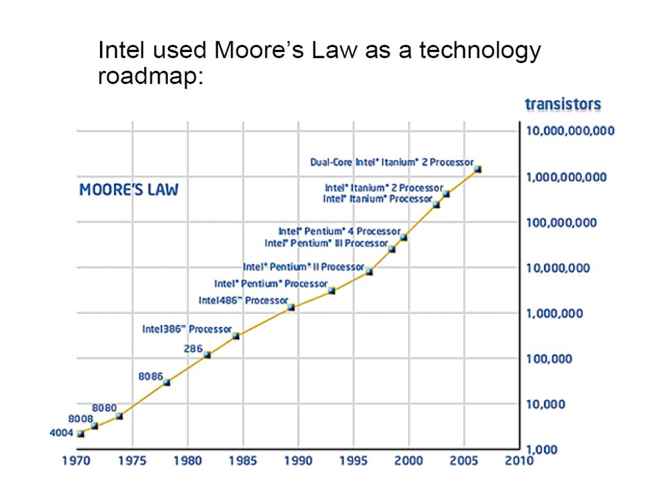
IC Integration Scales 12 In 1975, he updated his prediction to once every months.

19
Factors that contribute to the accuracy of Moore’s Law
Miniaturization size of transistor from 10µm (micron) to submicron. Nowadays, the smallest transistor is 45nm (0.045µm). Evolution of transistor design rule micron submicron deep submicron nano technology 10µm µm µm nm (Pentium Dual Core) 5µm µm µm 20nm (in research) 3µm µm µm
 to submicron. Nowadays, the smallest transistor is 45nm (0.045µm). Evolution of transistor design rule. micron submicron deep submicron nano technology. 10µm 1µm 0.18µm 45nm (Pentium Dual Core) 5µm 0.5µm 0.01µm 20nm (in research) 3µm 0.35µm 0.25µm.")
20
Factors that contribute to the accuracy of Moore’s Law
The law is still disputed because the linear growth starts to decline; the number of transistors should increase linearly, but it starts to decrease after 1970.

21
Microelectronics Evolution
Year Technology No. of transistors Example Transistor 1 - Discrete Component FET, Diode SSI - Small scale integration 10 Logic Gates, Flip-flop MSI - Medium scale integration 100 – 1000 Counter, Multiplexer LSI - Large scale integration 1000 – 20,000 RAM, Microprocessor VLSI - Very large scale integration 20,000 – 1,000,000 16 bits and 32 bits Microprocessor ULSI - Ultra large scale integration 1,000,000 – 10,000,000 Graphic microprocessor nowadays GSI - Giant scale integration > 10,000,000 Pentium Dual Core Microprocessor

22
Student Centred Activity - Group Discussion 1
Based on the given graphs, relate Moore’s Law to the following evolution of microelectronics memory devices. Based on the given graphs, relate Moore’s Law to the scaling down of transistor size and the trend in microprocessors.

23
Question # 1.

24
Question # 2

25
Classification of Integrated Circuit
In general, IC can be classified into FOUR (4) categories : Classification based on circuits function Classification based on the fabrication method Classification based on transistor type Classification based on design methodology
 categories : Classification based on circuits function. Classification based on the fabrication method. Classification based on transistor type. Classification based on design methodology.")
26
Classification Based on Fabrication Method
IC Classification based on fabrication method: a. Monolithic b. Film c. Hybrid

27
Classification Based on Fabrication Method
a. Monolithic The word ‘monolithic’ is derived from the Greek word monos, meaning ’single’ and lithos, meaning ‘stone’. A monolithic IC is a miniaturized electronic circuit including both active and passive components and their interconnections are being manufactured in the surface of a thin substrate of semiconductor material.

28
Monolithic IC

29
Monolithic IC Criteria of monolithic IC:
most popular because of low cost high reliability isolation weakness limited range of passive components circuit design is not flexible.

30
Classification Based on Fabrication Method
b. Film Film components are made of either conductive or nonconductive material that is deposited in desired patterns on a ceramic or glass substrate. Film can only be used as passive circuit components, such as resistors and capacitors. Transistors and/or diodes are added to the substrate to complete the circuit.

31
Film IC Plastic thin film Image on thin film

32
Classification Based on Fabrication Method
c. Hybrid IC Hybrid integrated circuit technology is the combination of monolithic circuits and film technology. The active components are monolithic transistors or diodes. The passive components may be group of monolithic resistors or capacitors on a single chip, or they may be thin-film components. Wiring or a metallized pattern provides connections between chips.

33
Hybrid IC Hybrids ICs are widely used for high power audio amplifier applications from 5 W to more than 50 W.

34
Hybrid IC Hybrid ICs usually have better performance than monolithic ICs. However, the process is too expensive for mass production. Thus, multi-chip techniques are quite economical for small quantity production and are more often used as prototypes for monolithic ICs.

35
Fabrication Method Comparison
Characteristics Monolithic Technology Film Technology Hybrid Technology Type of components Active and passive Passive (Resistor & Capacitor) Substrate material Silicon (Si) Germanium(Ge) Gallium Arsenide (GaAs) Conduction layer on insulator (glass, ceramic) Silicon and insulator Interconnection method On substrate surface Metal (Al or gold) Interconnection of two or more chips Technology method BJT, MOS,GaAs Thin film = 0.5m Thick film = 25m Combination of monolithic and film Size Medium Small Large
 Substrate material. Silicon (Si) Germanium(Ge) Gallium Arsenide (GaAs) Conduction layer on insulator (glass, ceramic) Silicon and insulator. Interconnection method. On substrate surface. Metal (Al or gold) Interconnection of two or more chips. Technology method. BJT, MOS,GaAs. Thin film = 0.5m. Thick film = 25m. Combination of monolithic and film. Size. Medium. Small. Large.")
36
Student Centred Activity - Group Discussion 2
Identify the advantages and disadvantage of Monolithic, Film and Hybrid fabrication methods.

37
Classification Based on Circuits Function
Integrated Circuits Linear / Analogue ICs Integrated circuits that operate with analogue signals at the input and output. Digital ICs Integrated circuits that operate with digital signals at the input and output. Examples: Op-Amp ii. Power Amplifier iii. Multiplier iv. Comparator v. Voltage Regulator Examples: i Logic gates ii. Flip-flop iii. Counter iv. Calculator chips v. Memory vi. Microprocessor

38
Classification Based on Transistor Types

39
Bipolar Junction Transistor (BJT)
NPN Cross section and Symbol PNP Cross section and Symbol

40
Advantage & Disadvantage of BJT ICs
Transistor Type Advantage Disadvantage BJT i. High switching speed High durability High power handling capability i. High power dissipation ii. Large chip size iii. Temperature sensitive

41
MOS IC MOS transistor is known as MOSFET (Metal Oxide Semiconductor Field-Effect Transistor). MOSFET is widely used nowadays in electronic equipment, e.g. mobile phone, computer, medical electronic equipment, etc. Examples of MOS technologies are: i. PMOS ii. NMOS iii. CMOS iv. VMOS

42
PMOS & NMOS PMOS Cross Section PMOS Symbol NMOS Cross Section
NMOS Symbol

43
Schematic diagram of 2-input NAND gate using CMOS
CMOS Cross Section Schematic diagram of 2-input NAND gate using CMOS 2-input NAND gate symbol

44
VMOS One of the disadvantages of CMOS technology is the disability of handling high power. VMOS is invented to overcome the problem. VMOS has the capability to operate in high current and voltage.

45
VMOS VMOS is the acronym of Vertical Metal Oxide Semiconductor.
VMOS has the V shape gate to conduct more carriers vertically from SOURCE to DRAIN. P + G S D

46
BiCMOS BiCMOS is the acronym of Bipolar complementary metal oxide semiconductor , the technology that combines BJT and CMOS on the same chip to generate high speed, low power dissipation and high concentration circuit.

47
Advantages & Disadvantages of MOS technology
MOS Transistor Types Advantage Disadvantage PMOS i. Low fabrication cost. ii. Simple fabrication method. Low circuit performance (slow). This is because the hole current mobility is two times slower than electron. NMOS i. Smaller size compared to PMOS. ii. High circuit performance. i. Fabrication process is more difficult compare to PMOS. CMOS i. Low power dissipation. Larger size compared to PMOS and NMOS. BiCMOS i. High circuit performance (high speed). ii. Low power dissipation. i. Larger chip size. ii. Complex fabrication process. iii. High fabrication cost. VMOS i. Capable of operating in high current and voltage. ii. High circuit performance (high speed). i. Complex fabrication process. ii. High fabrication cost.
. This is because the hole current mobility is two times slower than electron. NMOS. i. Smaller size compared to PMOS. ii. High circuit performance. i. Fabrication process is more difficult compare to PMOS. CMOS. i. Low power dissipation. Larger size compared to PMOS and NMOS. BiCMOS. i. High circuit performance (high speed). ii. Low power dissipation. i. Larger chip size. ii. Complex fabrication process. iii. High fabrication cost. VMOS. i. Capable of operating in high current and voltage. ii. High circuit performance (high speed). i. Complex fabrication process. ii. High fabrication cost.")
48
Student Centred Activity - Group Discussion 3
Distinguish Mixed-signal ICs from Analogue and Digital ICs. What do you think it is? Highlight the advantages and disadvantages of Mixed-Signal ICs. Reference:

49
Student Centred Learning - Group Discussion
Based on the given graphs, relate Moore’s Law to the following evolution of microelectronics memory devices. Based on the given graphs, relate Moore’s Law to the scaling down of transistor size and the trend in microprocessors. Distinguish Mixed-signal ICs from Analogue and Digital ICs. What do you think it is? Highlight the advantages and disadvantages of Mixed-Signal ICs. Reference: Advantages and disadvantage of Monolithic, Film and Hybrid fabrication methods.

50
Review of Learning Outcomes
At the end of this session, students should be able to: Understand Integrated Circuit (IC) Technology Know the classification of IC Have You Achieved the Outcomes?
 Technology. Know the classification of IC. Have You Achieved the Outcomes")
51
Lets see whether you have achieved the learning outcomes
Assessment Task QUIZ 1 (CLO1)
")
Similar presentations


>")


![EE314 Basic EE II Silicon Technology [Adapted from Rabaey’s Digital Integrated Circuits, ©2002, J. Rabaey et al.]](/16/5137281/big_thumb.jpg "EE314 Basic EE II Silicon Technology [Adapted from Rabaey’s Digital Integrated Circuits, ©2002, J. Rabaey et al.]>")

 Importance for LSI/VLSI –Low fabrication cost –Small size –Low power consumption Applications –Microprocessors –Memories.>")


 by Brattain with Bardeen providing the.>")
 1 SEMICONDUCTOR TECHNOLOGY -CMOS- Fire Tom Wada.>")