Download presentation
Presentation is loading. Please wait.

1
Ultra-fast differential front-end electronics
Detectors as signal generators ~ Overview Low Z vs High Z Front-End Electronics (FEE), Differential vs. single ended FEE, Preliminary design & measurements G. Pascovici, IKP-Cologne, FEE Meeting, Saclay, 04 Dec. 2008
, Differential vs. single ended FEE, Preliminary design & measurements. G. Pascovici, IKP-Cologne, FEE Meeting, Saclay, 04 Dec")
2
Front-end electronics – overview
Detector as a fast signal generator electron-hole pairs collection only electrons (or particles) Front-end Electronics preamplifier preamplifiers & shapers & comparators test system cooling and grounding Main requirements: gain (sensibility), dynamic range (directly and/or ToT), S/N, rise/fall time and/or counting rates, crosstalk, EMI, EMC, power consumption etc. G. Pascovici, IKP-Cologne, FEE Meeting, Saclay, 04 Dec. 2008
 Front-end Electronics. preamplifier. preamplifiers & shapers & comparators. test system. cooling and grounding. Main requirements: gain (sensibility), dynamic range (directly and/or ToT), S/N, rise/fall time and/or counting rates, crosstalk, EMI, EMC, power consumption etc. G. Pascovici, IKP-Cologne, FEE Meeting, Saclay, 04 Dec")
3
Detector Signal Collection
Circuit High Z Impedance adaptation Amplitude resolution Time resolution Noise cut Low Z Voltage source + Zo Rp Z - Low Z T Francis ANGHINOLFI ELEC-2005 Electronics in High Energy Physics Winter Term: Introduction to electronics in HEP Quo vadis ? Low Z output voltage source circuit can drive any load Output signal shape adapted to subsequent stage (ADC) Signal shaping is used to reduce noise (unwanted fluctuations) vs. signal
 Signal shaping is used to reduce noise (unwanted fluctuations) vs. signal.")
4
Front-end electronics – overview
Detector as fast signal generator electron-hole pairs collection only electrons (or particles) Z + - Detector Rp if Z is high charge is kept on capacitor nodes and voltage builds up (until capacitor is discharged) Advantages: - excellent E resolution - friendly pulse shape analysis Disadvantages: - channel-to-channel crosstalk - pile up above 40 k c.p.s. - sensitivity to e.m.c. FEE (Input stage) G. Pascovici, IKP-Cologne, FEE Meeting, Saclay, 04 Dec. 2008
 Z. + - Detector. Rp. if Z is high. charge is kept on capacitor nodes and voltage builds up (until capacitor is discharged) Advantages: - excellent E resolution. - friendly pulse shape analysis. Disadvantages: - channel-to-channel crosstalk. - pile up above 40 k c.p.s. - sensitivity to e.m.c. FEE. (Input stage) G. Pascovici, IKP-Cologne, FEE Meeting, Saclay, 04 Dec")
5
Front-end electronics – overview
Detector as fast signal generator electron-hole pairs collection only electrons (or particles) Z + - Detector Rp if Z is low charge flows as a current through the impedance in a short time. Advantages: - limited signal pile up - limited channel-to-channel crosstalk - low sensitivity to parasitic signals - good timing resolution Disadvantages: - pour signal/noise ratio FEE (Input stage) G. Pascovici, IKP-Cologne, FEE Meeting, Saclay, 04 Dec. 2008
 Z. + - Detector. Rp. if Z is low. charge flows as a current through the impedance in a short time. Advantages: - limited signal pile up. - limited channel-to-channel crosstalk. - low sensitivity to parasitic signals. - good timing resolution. Disadvantages: - pour signal/noise ratio. FEE. (Input stage) G. Pascovici, IKP-Cologne, FEE Meeting, Saclay, 04 Dec")
6
MRCP detectors for LHC

7
Front-end electronics – overview
Detector as fast signal generator electron-hole pairs collection only electrons (or particles) if Z is low charge flows as a current through the impedance in a short time. Advantages: - limited signal pile up - limited channel-to-channel crosstalk - low sensitivity to parasitic signals - good timing resolution Disadvantages: - pour signal/noise ratio Single ended structure
 if Z is low. charge flows as a current through the impedance in a short time. Advantages: - limited signal pile up. - limited channel-to-channel crosstalk. - low sensitivity to parasitic signals. - good timing resolution. Disadvantages: - pour signal/noise ratio. Single ended structure.")
8
Front-end electronics – overview
Specifications: Fully differential transimpedance 0.18µm standard CMOS techn. 10 GHz bandwidth dynamic range 25 µA -2.5 mA power consumption 88mW (2V)
")
9
Charge Sensitive Preamplifier
Active Integrator (“Charge Sensitive (Pre)Amplifier”) Input impedance very high ( i.e. NO signal current flows into amplifier), Cf (Rf) feedback capacitor (resistor) between output and input, very large equivalent dynamic capacitance, sensitivity A(q) ~ q / Cf, large open loop gain Ao ~ 10, ,000 Ci ~ “dynamic” input capacitance Rf G. Pascovici, IKP-Cologne, FEE Meeting, Saclay, 04 Dec. 2008
Amplifier ) Input impedance very high ( i.e. NO signal current flows into amplifier), Cf (Rf) feedback capacitor (resistor) between output and input, very large equivalent dynamic capacitance, sensitivity A(q) ~ q / Cf, large open loop gain Ao ~ 10, ,000. Ci ~ dynamic input capacitance. Rf. G. Pascovici, IKP-Cologne, FEE Meeting, Saclay, 04 Dec")
10
Standard Charge Sensitive preamplifiers developed at IKP Cologne et al.
Main achievements: low noise, fast preamplifiers (segmented HP-GE & DSSSD) clean transfer function pulse shape …(no over/under-shoots) differential outputs for HP-Ge detectors & DSSSD-Si high dynamic range highly accurate spectroscopic TOT method (up to ~200MeV) incorporated programmable pulser (50 ppm long term) cryostat wiring (cold part), crosstalk less then 10 miniature, SMD technology -3 Who are our main users? - large arrays of segmented HP-Ge detectors : Miniball (CERN), Rising (GSI), SeGa (MSU), Tigress (Triumf), AGATA (EU) - DSSD Si detectors: LuSia (Lund,GSI), LYCCA (GSI)… G. Pascovici, IKP-Cologne, FEE Meeting, Saclay, 04 Dec. 2008
 clean transfer function pulse shape …(no over/under-shoots) differential outputs for HP-Ge detectors & DSSSD-Si. high dynamic range. highly accurate spectroscopic TOT method (up to ~200MeV) incorporated programmable pulser (50 ppm long term) cryostat wiring (cold part), crosstalk less then 10. miniature, SMD technology. -3. Who are our main users - large arrays of segmented HP-Ge detectors : Miniball (CERN), Rising (GSI), SeGa (MSU), Tigress (Triumf), AGATA (EU) - DSSD Si detectors: LuSia (Lund,GSI), LYCCA (GSI)… G. Pascovici, IKP-Cologne, FEE Meeting, Saclay, 04 Dec")
11
Miniball HeKo basic structure
Advantages: discrete electronic components (e.g. HEMT, GaAs, SiGe) can be easily integrated, flexible open loop gain, frequency compensation vs. detector unfriendly wiring Disadvantages: to low open-loop gain larger size G. Pascovici, IKP-Cologne, FEE Meeting, Saclay, 04 Dec. 2008
 can be easily integrated, flexible open loop gain, frequency compensation vs. detector unfriendly wiring. Disadvantages: to low open-loop gain. larger size. G. Pascovici, IKP-Cologne, FEE Meeting, Saclay, 04 Dec")
12
Charge Sensitive Loop - basic structure
LYCCA CSPs Charge Sensitive Loop - basic structure Advantages: the use of advanced current feedback operational amplifier, very fast, compact, small size, low PS Disadvantages: to large open-loop gain, limited frequency compensation vs. detector unfriendly wiring G. Pascovici, IKP-Cologne, FEE Meeting, Saclay, 04 Dec. 2008

13
G. Pascovici, IKP-Cologne, FEE Meeting, Saclay, 04 Dec. 2008
GALI -S66 (GSI) G. Pascovici, IKP-Cologne, FEE Meeting, Saclay, 04 Dec. 2008
 G. Pascovici, IKP-Cologne, FEE Meeting, Saclay, 04 Dec")
14
AGATA Single & Dual Gain Core reworked frequency compensations
internal network compensation Lead comp. (1. OpAmp) Cryostat wiring as part of the front-end electronics external network compensation - minimum Miller effect (min.) - lead compensation (min.) - lead-lag compensation (adj.) - dominant pole compensation (adj.)
 Cryostat wiring as part of the front-end electronics. external network. compensation. - minimum Miller effect (min.) - lead compensation (min.) - lead-lag compensation (adj.) - dominant pole compensation (adj.)")
15
LYCCA CSPs (32- channels) block diagram - basic structure
Input: 68x high density flat band cable (SE*GND) Output: 32x Differential 100 Ohm*, 68x high density flat band cable x 32 channels G. Pascovici, IKP-Cologne, FEE Meeting, Saclay, 04 Dec. 2008
 Output: 32x Differential 100 Ohm*, 68x high density flat band cable. x 32 channels. G. Pascovici, IKP-Cologne, FEE Meeting, Saclay, 04 Dec")
16
tr ~ 18 ns (Gain x1; Cd~10pF) LYCCA - CSPs Transfer Function
a) energy channel (differential out.) tr ~ 18 ns (Gain x1; Cd~10pF) tr ~ 29 ns (Gain x3; Cd~10pF) b) up-graded time channels (also with differential outputs) tr ~ 200 pS (tentative) LYCCA CSPs 200 MeV & 4 GeV 32 channels only with energy diff. outputs or 16 channels with both, energy and ultra fast diff. outputs mean min max
 energy channel (differential out.) tr ~ 18 ns (Gain x1; Cd~10pF) tr ~ 29 ns (Gain x3; Cd~10pF) b) up-graded time channels. (also with differential outputs) tr ~ 200 pS (tentative) LYCCA CSPs. 200 MeV & 4 GeV. 32 channels only with. energy diff. outputs. or. 16 channels with both, energy and ultra fast. diff. outputs. mean. min. max.")
17
Sub - nanosecond CSP GaAs – HEMT ultra-fast, narrow time output
(Q1, Q2) ultra-fast, narrow time output (note: measured with existing scopes: tr ~ 500 ps, expected tr ~ 200ps !) energy output tf~10 µs (no P/Z cancellation) high counting rates timing > ~1 Mcps dominant pole compensation included low power, only +/- 6V E +/- 3V T) G. Pascovici, IKP-Cologne, FEE Meeting, Saclay, 04 Dec. 2008
 ultra-fast, narrow. time output. (note: measured with. existing scopes: tr ~ 500 ps, expected tr ~ 200ps !) energy output tf~10 µs. (no P/Z cancellation) high counting rates. timing > ~1 Mcps. dominant pole. compensation included. low power, only +/- 6V E. +/- 3V T) G. Pascovici, IKP-Cologne, FEE Meeting, Saclay, 04 Dec")
18
LYCCA CSP modified for fast timing outputs: jFET: Bf861; BF862,
HEMT: ATF-55143 Id ~ from 2mA – 10 mA

19
Idrain, Vdrain to optimize the
tr ~ 720 ps jFET, FET, HEMT selection a) jFET, FET BF861 (1,B,C); BF862; BF 889 b) GaAs-FETs (E-pHEMT) ATF-35143; ATF-55143; ATF-38143 Idrain, Vdrain to optimize the noise & bandwidth characteristics (10-15 mA, V, 20-30mW) Pulse generator: Tektronix PG502 modified (less than 700ps rise/fall time) Scope: Tektronix TDS 3032 (300 MHz, 2.5 GHz sampling) tr ~ 930 ps
 jFET, FET. BF861 (1,B,C); BF862; BF 889. b) GaAs-FETs (E-pHEMT) ATF-35143; ATF-55143; ATF Idrain, Vdrain to optimize the. noise & bandwidth characteristics. (10-15 mA, V, 20-30mW) Pulse generator: Tektronix PG502 modified. (less than 700ps rise/fall time) Scope: Tektronix TDS (300 MHz, 2.5 GHz sampling) tr ~ 930 ps.")
20
Idrain, Vdrain to optimize the
jFET, FET, HEMT selection a) jFET, FET BF861 (1,B,C); BF862; BF 889 b) GaAs-FETs (E-pHEMT) ATF-35143; ATF-55143; ATF-38143 Idrain, Vdrain to optimize the noise & bandwidth characteristics (10-15 mA, V, 20-30mW) tr ~ 505 ps Pulse generator: Tektronix PG502 modified (less than 700ps rise/fall time) Scope: LeCroy 44Xs (400 Mhz, 2.5 GHz sampling) tr ~ 499 ps
 jFET, FET. BF861 (1,B,C); BF862; BF 889. b) GaAs-FETs (E-pHEMT) ATF-35143; ATF-55143; ATF Idrain, Vdrain to optimize the. noise & bandwidth characteristics. (10-15 mA, V, 20-30mW) tr ~ 505 ps. Pulse generator: Tektronix PG502 modified. (less than 700ps rise/fall time) Scope: LeCroy 44Xs. (400 Mhz, 2.5 GHz sampling) tr ~ 499 ps.")
21
Idrain, Vdrain to optimize the tf ~ 498 ps
jFET, FET, HEMT selection a) jFET, FET BF861 (1,B,C); BF862; BF 889 b) GaAs-FETs (E-pHEMT) ATF-35143; ATF-55143; ATF-38143 Idrain, Vdrain to optimize the noise & bandwidth characteristics (10-15 mA, V, 20-30mW) tf ~ 498 ps Pulse generator: Tektronix PG502 modified (less than 700ps rise/fall time) Scope: LeCroy 44Xs (400 Mhz, 2.5 GHz sampling) tf ~ 498 ps G. Pascovici, IKP-Cologne, FEE Meeting, Saclay, 04 Dec. 2008
 jFET, FET. BF861 (1,B,C); BF862; BF 889. b) GaAs-FETs (E-pHEMT) ATF-35143; ATF-55143; ATF Idrain, Vdrain to optimize the. noise & bandwidth characteristics. (10-15 mA, V, 20-30mW) tf ~ 498 ps. Pulse generator: Tektronix PG502 modified. (less than 700ps rise/fall time) Scope: LeCroy 44Xs. (400 Mhz, 2.5 GHz sampling) tf ~ 498 ps. G. Pascovici, IKP-Cologne, FEE Meeting, Saclay, 04 Dec")
22
position sensitive detector
Read-out from a MCP + dual delay line based position sensitive detector Two mutually perpendicular delay lines * - Sobottka & Williams, IEEE Trans. NS (1988),35, p348 - Kozulin, Kondratiev et al.,Nucl.Exp.Tech., 2008 No 58, p.44-58 Preliminary design - test measurements
,35, p Kozulin, Kondratiev et al.,Nucl.Exp.Tech., No 58, p Preliminary design - test measurements.")
23
Read-out from a MCP-based position sensitive detector
LT6411 3300V/µs 650 MHz mW / ch. G. Pascovici, IKP-Cologne, FEE Meeting, Saclay, 04 Dec. 2008

24
LYCCA CSPs (32- channels) block diagram - basic structure
Input: 68x high density flat band cable (SE*GND) Outputs: 32x E - differential 100 Ohm*, 68x high density flat band cable x 32 channels G. Pascovici, IKP-Cologne, FEE Meeting, Saclay, 04 Dec. 2008
 Outputs: 32x E - differential 100 Ohm*, 68x high density flat band cable. x 32 channels. G. Pascovici, IKP-Cologne, FEE Meeting, Saclay, 04 Dec")
25
LYCCA like CSPs with implemented ultra-fast
differential time outputs – 16x channels Input: 68x high density flat band cable (SE*GND) Outputs: 16x [E] ch. - differential 100 Ohm*, 32E out of 68 x high density flat band cable (10µs) (a) Diff. Comp. CML, LV-PECL, LVDS (b) tf ~10ns* (opt. ~ 100ns) Outputs: 16x [T] ch. - differential 100 Ohm*, 32T out of 68x high density flat band cable x 16 channels G. Pascovici, IKP-Cologne, FEE Meeting, Saclay, 04 Dec. 2008
 Outputs: 16x [E] ch. - differential 100 Ohm*, 32E out of 68 x high density flat band cable. (10µs) (a) Diff. Comp. CML, LV-PECL, LVDS. (b) tf ~10ns* (opt. ~ 100ns) Outputs: 16x [T] ch. - differential 100 Ohm*, 32T out of 68x high density flat band cable. x 16 channels. G. Pascovici, IKP-Cologne, FEE Meeting, Saclay, 04 Dec")
26
To be decided: - with TOT ?
- with spectroscopic TOT ? - differential signals standard: PECL, NECL, CML ?

27
To be decided: - with TOT ? And where ? On [E] or on [T] channel ?
- with spectroscopic TOT ? Or quasi spectroscopic? - differential signals standard: PECL, NECL, CML ? TOT circuitry? - requirements has to be decided ? - E or/and T ch.?
![To be decided: - with TOT And where On [E] or on [T] channel](http://slideplayer.com/slide/10276347/34/images/27/To+be+decided%3A+-+with+TOT+And+where+On+%5BE%5D+or+on+%5BT%5D+channel.jpg "- with spectroscopic TOT Or quasi spectroscopic - differential signals standard: PECL, NECL, CML TOT circuitry - requirements has. to be decided - E or/and T ch.")
28
~450 mW/ch + jFET 1 or 2 stages ~60 mW/ch + jFET
GaAs(HEMT) +Transimpedance preamplifier-amplifier ~450 mW/ch + jFET 1 or 2 stages GaAs(HEMT) +Si-Ge amplifier+ Si-Ge ultrafast comparator ~60 mW/ch + jFET
 +Transimpedance preamplifier-amplifier. ~450 mW/ch. + jFET. 1 or 2 stages. GaAs(HEMT) +Si-Ge amplifier+ Si-Ge ultrafast comparator. ~60 mW/ch. + jFET.")
29
Potential solution with “motherboard”
LYCCA architecture (8 -16 channels) Potential solution without “motherboard” Input Output architecture (2 - 4 channels) Ch1- timing Ch. 1 output Ch. 1 input Ch. 2 input Ch. 2 output Ch2- timing Advantages: very fast compact, small size low PS (450mW/ch) Disadvantages: power consumption in vacuum ? motherboard architecture impedance matching for UHF ? w. motherboard cooling in vacuum (~ 2D structure) no motherboard architecture impedance matching for UHF solution only for small number of channels, distribution of infrastructure signals (PS, adj.) no motherboard
 Potential solution without motherboard Input Output architecture (2 - 4 channels) Ch1- timing. Ch. 1. output. Ch. 1. input. Ch. 2. input. Ch. 2. output. Ch2- timing. Advantages: very fast. compact, small size. low PS (450mW/ch) Disadvantages: power consumption in vacuum motherboard architecture. impedance matching for UHF w. motherboard. cooling in vacuum (~ 2D structure) no motherboard architecture. impedance matching for UHF. solution only for small number of channels, distribution of infrastructure signals (PS, adj.) no motherboard.")
30
Sensitivity: A(t) ~100 mV/10 fC
slope: [ walk ] dynamic range, even for constant rise/fall times CFD, ELD (extrapolated leading edge), ARC correlated 2. channel [ jitter ] intrinsic noise, intrinsic jitter noise distribution bandwidth Timing jitter Intrinsic jitter Ratio: amplifier rise time/ collection time intrinsic jitter BW[Hz] bandwidth, Nd ~spectral density noise dispersion intrinsic time resolution M. Ciobanu et al, A FEE card comprising a high-gain amplifier and a fast discriminator for TOF measurements
, ARC. correlated 2. channel. [ jitter ] intrinsic noise, intrinsic jitter. noise distribution. bandwidth. Timing jitter. Intrinsic. jitter. Ratio: amplifier rise time/ collection time. intrinsic jitter. BW[Hz] bandwidth, Nd ~spectral density. noise dispersion. intrinsic time resolution. M. Ciobanu et al, A FEE card comprising a high-gain. amplifier and a fast discriminator for TOF measurements.")
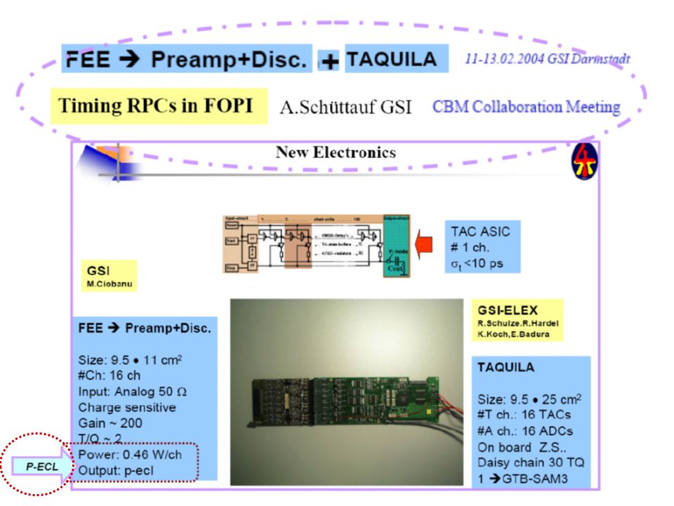
31
IE1I+IE2I

34
LVDS, CML differential interfaces common-mode range compared to
Electronic Design, Vol.46, No.25,1988 LVDS, CML differential interfaces common-mode range compared to single-ended noise margin. The effective noise margin is 2 to 4 times better using LVDS, CML…

Similar presentations

 CRYODET Workshop LNGS, 13-14 March 2006.>")


: basics>")


