Download presentation
Presentation is loading. Please wait.

1
The ILD ECAL Jan 28-30 th 2010 ILDWS @ Paris Satoru Uozumi (Kyungpook Natl. Univ.) for the ILD ECAL group
 for the ILD ECAL group.")
2
The ILD ECAL Finely granular PFA calorimeter with tungsten absorber Cell-size in baseline design ~ 5 x 5 mm 2, num. of cells ~100M in total Necessary to achieve less dead space, low production cost Candidate technologies : Silicon-tungsten Scintillator-tungsten MAPS/DECAL Jet Energy Resolution by M. Thomson Barrel: 5 octogonal wheels R min = 1808 mm; R max = 2220 mm Width = 940 mm End-caps: 4 quarters ∅ min = 800 mm

3
Silicon-tungsten ECAL ILD Structure – 20 layers of 2.1 mm (0.6X 0 ) W + 9 layers of 4.2mm (1.2X 0 )W – 5x5 mm 2 granularity of Si ~ 108 M cells in total 10x10 mm 2 physics prototype tested in beam – Energy resolution measured in test beam ~ 16.6%/√E(GeV) ⊕ 1.1% with S/N ratio of 7.5 for a mip signal – CERN (2006, 2007), FNAL (2008) Remaining hardware R&D issues – Power pulsing of FE electronics (common issue also for Sci ECAL) – Si sensor cost reduction … need 3000 m 2, current price 10 euro/cm 2
 W + 9 layers of 4.2mm (1.2X 0 )W – 5x5 mm 2 granularity of Si ~ 108 M cells in total 10x10 mm 2 physics prototype tested in beam – Energy resolution measured in test beam ~ 16.6%/√E(GeV) ⊕ 1.1% with S/N ratio of 7.5 for a mip signal – CERN (2006, 2007), FNAL (2008) Remaining hardware R&D issues – Power pulsing of FE electronics (common issue also for Sci ECAL) – Si sensor cost reduction … need 3000 m 2, current price 10 euro/cm 2")
4
Scintillator-tungsten ECAL Cost-effective scintillator strip calorimeter aiming to have virtual cells by x-y strips crossing. Beam tests of the physics prototype have been performed to prove feasibility. – DESY 2007 (small prototype) – FNAL 2008, 2009 (test with AHCAL) ILD structure – Scintillator strips with 5 mm width 2 mm thick without WLS fiber – 3 mm tungsten, ~21 X 0 in total Study of “strip-clustering” underway with realistic simulation Remaining Hardware R&D issues : – Study of 5 mm width scintillator-strip without WLS fiber – Dynamic range of photo-sensor – Establish design of the photo-sensor gain calibration system Scintillator strip (4.5 x 1 x 0.3 cm) MPPC WLS fiber 18 cm 72 strips x 30 layers
 – FNAL 2008, 2009 (test with AHCAL) ILD structure – Scintillator strips with 5 mm width 2 mm thick without WLS fiber – 3 mm tungsten, ~21 X 0 in total Study of strip-clustering underway with realistic simulation Remaining Hardware R&D issues : – Study of 5 mm width scintillator-strip without WLS fiber – Dynamic range of photo-sensor – Establish design of the photo-sensor gain calibration system Scintillator strip (4.5 x 1 x 0.3 cm) MPPC WLS fiber 18 cm 72 strips x 30 layers.")
5
MAPS (DECAL) option Potential large cost reductions – Standard CMOS sensor – No proprietary processes – Electronics all on sensor, reduced fabrication/assembly costs Ultimate spatial resolution – 50x50 μm 2 pixels – “TERA Pixel” detector TPAC readout chip v1.0-v1.2 = 168 x 168 pixels; 79.4 mm 2 Expected resolution (pixel counting) 13%/√E(GeV) ⊕ 1% Status: – successful CERN TB of 6 sensors summer 2009 – New SPiDeR collaboration – Physics prototype planned for 2012 Critical points – integration, Power consumption, services – Funding issue for further R&D
 option Potential large cost reductions – Standard CMOS sensor – No proprietary processes – Electronics all on sensor, reduced fabrication/assembly costs Ultimate spatial resolution – 50x50 μm 2 pixels – TERA Pixel detector TPAC readout chip v1.0-v1.2 = 168 x 168 pixels; 79.4 mm 2 Expected resolution (pixel counting) 13%/√E(GeV) ⊕ 1% Status: – successful CERN TB of 6 sensors summer 2009 – New SPiDeR collaboration – Physics prototype planned for 2012 Critical points – integration, Power consumption, services – Funding issue for further R&D")
6
Question from IDAG Each validated detector group will produce a detailed baseline design by 2012. To this end the following steps are planned. 1.Demonstrate proof principle on critical components. – When there are options, at least one option for each subsystem will reach a level of maturity which verifies feasibility. 2.Define a feasible baseline design. – While a baseline will be specified, options may also be considered 3.Complete basic mechanical integration of the baseline design accounting for insensitive zones such as the beam holes, support structure, cables, gaps or inner detector material. 4.Develop a realistic simulation model of the baseline design, including the identified faults and limitations.

7
Possible Idea for baseline design of the ILD ECAL A lot of discussion has been done to form the “Unified ILD ECAL” in this month. One possible idea is a “hybrid-type ECAL” with silicon pads and Scintillator-strips. – The silicon pads in pre-shower and shower-max region – The scintillator layers cover after the shower maximum – Another idea : Si layers interleaved in scintillator layers – Cost-effective – No two-fold ambiguity for the strip clustering with silicon sensors – Can use established the silicon and Scintillator ECAL technologies. – Need extensive simulation study to determine configuration of Silicon / Scintillator layers – Specific cell & strip combined clustering must be developed. Mokka simulation of the hybrid-type ECAL is under preparation. Two-fold ambiguity with strip clustering Si pads (5x5 mm 2 ) Scint strips (5-10 x 45 mm 2 )
 Scint strips (5-10 x 45 mm 2 ).")
8
Question from IDAG Each validated detector group will produce a detailed baseline design by 2012. To this end the following steps are planned. 1.Demonstrate proof principle on critical components. – When there are options, at least one option for each subsystem will reach a level of maturity which verifies feasibility. 2.Define a feasible baseline design. – While a baseline will be specified, options may also be considered The Silicon-Scintillator hybrid ECAL could be the possible candidate in case of problem with silicon cost or reconstruction problem of scintillator. This possibility is subject to study in next 2 years. MAPS pixels for digital ECAL under investigation as an option beyond the baseline. 3.Complete basic mechanical integration of the baseline design accounting for insensitive zones such as the beam holes, support structure, cables, gaps or inner detector material. 4.Develop a realistic simulation model of the baseline design, including the identified faults and limitations.

9
Question from IDAG Each validated detector group will produce a detailed baseline design by 2012. To this end the following steps are planned. 1.Demonstrate proof principle on critical components. – When there are options, at least one option for each subsystem will reach a level of maturity which verifies feasibility. 2.Define a feasible baseline design. – While a baseline will be specified, options may also be considered 3.Complete basic mechanical integration of the baseline design accounting for insensitive zones such as the beam holes, support structure, cables, gaps or inner detector material. 4.Develop a realistic simulation model of the baseline design, including the identified faults and limitations.

10
Major Milestones to prove Si-Sci-W ECAL feasibility by end 2012 Technical points - Produce short detector slab for both Silicon and Scintillator layers (by mid 2011) test it with cosmics and beams - Produce long Silicon detector slab (over ~1.5m) to test signal integrity etc. (by end 2011) - Demonstrate power pulsing of FE chips - First with single chip, short slabs of Si / Sci layers (by mid 2011) - Then with long slab (by end 2011) - Test in the magnetic field (by mid 2012) - Analysis of past test beam data, comparison with simulation (ongoing, ASAP) - Establish 5 mm width scintillator strip (by ~ 2010/2011) - Design and produce thin PCB for scintillator/MPPC layers (by mid 2011)
 - Demonstrate power pulsing of FE chips - First with single chip, short slabs of Si / Sci layers (by mid 2011) - Then with long slab (by end 2011) - Test in the magnetic field (by mid 2012) - Analysis of past test beam data, comparison with simulation (ongoing, ASAP) - Establish 5 mm width scintillator strip (by ~ 2010/2011) - Design and produce thin PCB for scintillator/MPPC layers (by mid 2011).")
11
Major Milestones to prove Si-Sci-W ECAL feasibility by end 2012 (cont’d) Simulation (all by mid 2010) - Implement dead zones of scintillator (photo-sensor, covering films) - Implement non-uniformity of strip response - Update ILD Si simulation to same level as CALICE SiW testbeam simulation - Implementation of service inside gap between barrel and end-cap Reconstruction - Realistic digitization (end-of-slab instrumentation, MPPC saturation) (by end 2010) - Clustering with strip and hybrid geometries (by mid 2011) - Study of PFA performance in different configurations of Si-Sci hybrid ECAL (by end 2011) MPPC Strip Strip response (ADC counts) Position along the strip (cm) Detector calibration - Define ILD ECAL calibration procedure (by end 2011)
 Simulation (all by mid 2010) - Implement dead zones of scintillator (photo-sensor, covering films) - Implement non-uniformity of strip response - Update ILD Si simulation to same level as CALICE SiW testbeam simulation - Implementation of service inside gap between barrel and end-cap Reconstruction - Realistic digitization (end-of-slab instrumentation, MPPC saturation) (by end 2010) - Clustering with strip and hybrid geometries (by mid 2011) - Study of PFA performance in different configurations of Si-Sci hybrid ECAL (by end 2011) MPPC Strip Strip response (ADC counts) Position along the strip (cm) Detector calibration - Define ILD ECAL calibration procedure (by end 2011)")
12
Milestones to prove MAPS DECAL option feasibility by end 2012 Technical – individual sensor characterization – Measure MIP efficiency from 2009/10 test beams for sensor variants – by end 2010 Including epitaxial layer dependence: deep P-well; high resistivity; layer thickness – Publish essential characterisation data – by end 2010 Pedestals; noise; response uniformity; trimming; calibration with 55 Fe; diffusion time – Comparison of shower densities in data and simulation - DESY testbeam, March 2010 Electron response and core shower density Results vs. particle energy and vs. material depth Single most critical result for DECAL – by early 2011 – Soft photon response downstream of absorber Simulation – Resolution of realistic DECAL to photons – by end 2010 Study dependence on pixel size; noise; deep P-well; charge diffusion; dead areas, etc. – Maintain compatibility with SiW analogue geometry/mechanics where appropriate, as expected for a high performance/lower cost option Reconstruction – Single particle and PFA tuned for DECAL in performance benchmark studies with most complete simulations – by end 2011

13
The EUDET prototype Silicon module Scintillator module The EUDET alveolar structure can accommodate both Si / Sci ECAL modules. Discussion underway to make the compatible structure. PCB Heat shield Scintillator W slab Photo-sensor Construction of the mechanical structure by end-2010. Implement detector modules ~ mid 2011. Future beam tests from ~ 2012 - Si + Sci module test - Validate power pulsing - Test simulation with finer granularity

14
Summary Technologies and feasibility for the ILD ECAL is being established (in the CALICE collaboration). – Several beam test has been done with SiW and SciW ECAL prototypes during 2006-2009. – Realistic simulation study with PandoraPFA is ongoing. Now those technologies are being unified to an idea of the hybrid-ECAL with the silicon and scintillator layers. – It could be a possible candidate of the ILD ECAL baseline design. – Extensive simulation study will be done in next 2 years. MAPS pixels for digital ECAL under investigation as an option beyond the baseline design. Still a lot of works need be addressed to finish homework given by IDAG. EUDET technical prototype will be the next stage of the hardware R&D. – Several tests will be running from 2010 until the DBD.

15
Backups

16
Silicon-tungsten R&D status Results of 2006 beam test @ CERN with 2/3 equipped SiW-ECAL – Highly linear response – Good energy / spatial resolution Analysis of 2007 and 2008 beam test data with fully equipped SiW-ECAL currently ongoing. SiW-ECAL AHCAL TCMT

17
Silicon-W issues for future R&D Other R&D issues : power pulsing of FE electronics Si sensors price (3000 m 2 ) currently 10 Euro/cm 2 Dips observed in ECAL response by inter-wafer gaps. Correction works, but dips cannnot fully recovered.

18
The EUDET ECAL prototype

19
Scintillator-ECAL strip clustering (with Mokka +Pandora PFA) Strip clustering with the scntillator-ECAL to make virtual cells from the strip geometry. Study of the strip clustering extensively underway Current result indicates that the JER doesn’t depend on the shape of the scintillator, but just changes with its area. Due to the two-fold ambiguity ? If so, adding small-pixel layer may resolve it.

20
Issues for the FE Electronics R&D PCB thickness < 1.2mm to fit into the EUDET structure Next SKIROC2 chip will be submitted for manufacture this month Main issue of the test is demostrating the power pulsing - Test with a single chip in a lab will start soon - Then it will be again tested in the detector slab - Also need the test inside B-field to check effect to the changing current.

21
The Scintillator-strip Structure and Readout Scintillator strip (4.5 x 1 x 0.2 cm) MPPC WLS fiber Strips made by extrusion. Baseline design … 1 x 4.5 cm strip 5 mm strip also feasible, further R&D necessary. Direct readout option w/o fiber is also being explored.

22
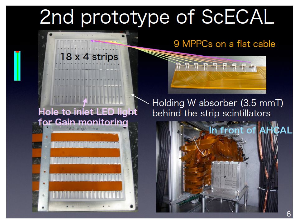
Calibration System of Photo-sensor Gain Light distribution system is designed to monitor the photo- sensor gain. Photons from LED are distributed into each scintillator through a notch on a fiber. First system is designed and tested with the 2 nd ScECAL prototype. MPPC output (ADC counts) LED Notches
 LED Notches.")
23
Response calibration by MIP Need to calibrate response of each individual strip using Minimum Ionizing Particle (MIP). To do that, one possibility is utilizing hadrons in jets as MIPs. Simulation result indicates calibration within + 5 % accuracy is possible with 2-3 days running at high luminosity Z-pole running. Select isolated MIPs In jets Strip response Center-of-mass energyDays to take +5% calibration 91.2 GeV2-3 days 200 GeV400 days 500 GeV2500 days

24
ScECAL Geometry Total thickness 172 mm, corresponds to 20.6X 0. ~10M channels in total (case for 1 x 4 cm strip) 3 mm tungsten + 2 mm scintillator-strips + 2 mm readout/service
 3 mm tungsten + 2 mm scintillator-strips + 2 mm readout/service.")
Similar presentations


 at EUDET Telescope Sensor overview with lab results –TPAC –FORTIS.>")


 Roman Poschl (LAL Orsay)>")


 on behalf of the CALICE collaboration.>")
 Temperature & Voltage Dependence Option 2: Optical system Option 2: LED driver Calibration of the Hadronic Calorimeter Prototype.>")
 for the GLD calorimeter group We are planning to have two beam.>")

 May-31 2008 Japan-Korea meeting.>")

 STFC funded us for £75k/year travel money in 2015 and 2016 to re->")