Download presentation
Presentation is loading. Please wait.

1
MCH(Muon Tracking) DCS Introduction Overview drawing High Voltage - hardware functional diagram Logical Diagrams Summary table of states and commands Commands from DCS and State Diagrams Proposal for hardware partitioning of the HV Modules Proposal of some PVSS2 panels
 DCS Introduction Overview drawing High Voltage - hardware functional diagram Logical Diagrams Summary table of states and commands Commands from DCS and State Diagrams Proposal for hardware partitioning of the HV Modules Proposal of some PVSS2 panels")
2
Introduction The ultimate goal is a working Detector Control System (DCS) ready for exploitation, allowing to control and operate the experiment during all modes of operation and according to defined requirements. The Control Systems for Tracking chambers detector should be ready to be used during the final assembly and commissioning. The main parties involved in the DCS project are the various detector groups and the groups providing the external services. In addition the ECS and Offline systems as well as the LHC Machine need to be linked-up with DCS. The control and operation of the experiment takes place on the ECS layer. Through this layer DCS is linked up with the Data Acquisition (DAQ), Trigger (TRG) and Offline systems and with the LHC Machine(fig.1).
, Trigger (TRG) and Offline systems and with the LHC Machine(fig.1)..")
3
Fig. 1 Experimental Control System

4
DCS layout The ‘standard’ DCS model consists of a number of hardware and software components on three hierarchical layers: the supervision layer, the control layer and the field layer. Supervision layer (PVSS2, Framework) The supervision and operation of the detectors take place on this layer and some of the tools and facilities needed are: -SCADA framework tools (PVSS2,Framework) -logging and archiving facilities -alarms -configuration databases -application programs and data -object library for supervision -supervision and operation programs (Finite State Machines)
 The supervision and operation of the detectors take place on this layer and some of the tools and facilities needed are: -SCADA framework tools (PVSS2,Framework) -logging and archiving facilities -alarms -configuration databases -application programs and data -object library for supervision -supervision and operation programs (Finite State Machines).")
5
Control layer On the control layer the collection and processing of data takes place and the following components can typically be found here: - Process Control Units - Local Operator Workplace - Local Engineering Workplace - Data server - Application programs and data - Object library for process control - Local operation programs - Sub-detector configuration data Field layer The connection of the detector equipment to DCS takes place on the field layer via sensors, I/O-interfaces, OPC servers and fieldbuses.

6
ALICE policy: Our baseline approach is to build the ALICE DCS as a distributed PVSS system Each detector DCS shall be a distributed PVSS system “Central DCS” will connect to all PVSS systems –Distributed system of distributed systems

7
ACC CR4-X01 Detector PVSS II Detector Ethernet Database(s) OPC client DIM client 344600 Detector ? High VoltageLow VoltageEnvironment monitor User interface PVSS II E HV LV Muon-Trk Control room (ACR) [FSM] FEE/Crate Control 27/06/05 HV Switch 188 HV S 1 Crocus (on-detector crates) DDL 48 Geometry monitor Geometry 40 “FED” to ‘driver boards’; DIM to ‘Analysis system’ CR3 CAEN OPC PVSS II OPC client RS485 repeater 1402 CR4-Z05 SY1527 2 UX-D Wiener 30 E CR3 Wiener OPCserver PVSS II OPC client E E CR3 [GMS] DIMserver DIMclient CR3 PVSS II DIMclient Driver boards ELMB (I/O device) CR3 PCI-CAN ELMB OPCserver PVSS II OPC client C 11..4 CR3 SG2 CR5 SG2 Gas system PLC Gas E Detector PVSS II DIP [GWG] Gas Gas PVSS UX-C CR3 Cooling (air or water) PLC Detector Cooling E Detector PVSS II Modbus/TCP 1 [TS/CV] TS/CV SCADA 20122 Modbus OPC
 [FSM] FEE/Crate Control 27/06/05 HV Switch 188 HV S 1 Crocus (on-detector crates) DDL 48 Geometry monitor Geometry 40 FED to ‘driver boards’; DIM to ‘Analysis system’ CR3 CAEN OPC PVSS II OPC client RS485 repeater 1402 CR4-Z05 SY UX-D Wiener 30 E CR3 Wiener OPCserver PVSS II OPC client E E CR3 [GMS] DIMserver DIMclient CR3 PVSS II DIMclient Driver boards ELMB (I/O device) CR3 PCI-CAN ELMB OPCserver PVSS II OPC client C CR3 SG2 CR5 SG2 Gas system PLC Gas E Detector PVSS II DIP [GWG] Gas Gas PVSS UX-C CR3 Cooling (air or water) PLC Detector Cooling E Detector PVSS II Modbus/TCP 1 [TS/CV] TS/CV SCADA Modbus OPC.")
8
Operator Node HV(HVLV Left) LV(HVLV Right) ELMB (Environment) +GMS Computers for Muon Trk DCS
 LV(HVLV Right) ELMB (Environment) +GMS Computers for Muon Trk DCS")
9
OFFLINE The DCS Data FlowConfig. PVSSII Archive ECS Electricity Ventilation Cooling Gas Magnets Safety Access Control LHC DAQTRIHLT DIM, DIP FERO Version Tag Devices Devices Devices Devices Conditions AMANDA

10
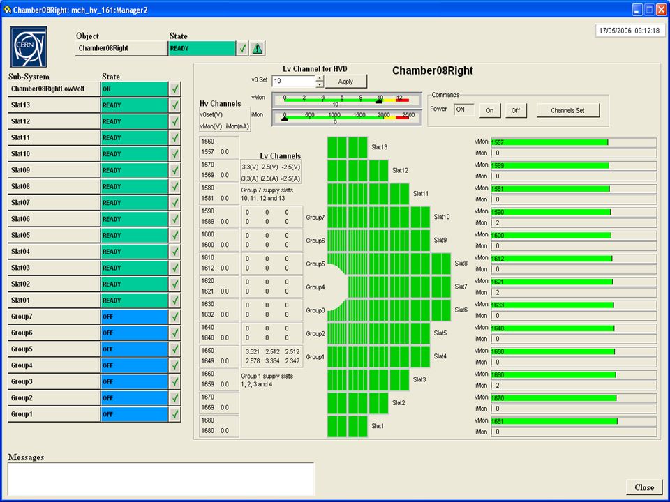
Cb5LCb6L ST1 High Voltage Power Supply cable ST3ST4 ST5 IP RIGHT LEFT Cb5RCb6R TOP VIEW hvd13 hvd1 hvd3 hvd9 hvd7 hvd1 hvd2 hvd9 hvd5 SY1527 LEFT 8xA1821HP CR04-Z05 PC DCS USB RS485 CR03-Z06 ST2 Cb - Chamber (ex. Cb1L – Chamber # 1 Left) hvd3 hvd5 hvd7 hvd8 hvd4 hvd6 hvd2 hvd8 hvd4 hvd6 hvd2 hvd12 hvd1 hvd13 hvd2 hvd12 hvd1 hvd13 hvd2 hvd12 hvd1 hvd13 hvd2 hvd12 hvd1 Cb7LCb8L Cb9L Cb10L Cb10RCb9RCb7RCb8R High Voltage 6666 Cb1L Cb2L Cb3L Cb4L Cb1R Cb2R Cb3R Cb4R 99 SY1527 RIGHT 8xA1821HP ST - Station 13
 hvd3 hvd5 hvd7 hvd8 hvd4 hvd6 hvd2 hvd8 hvd4 hvd6 hvd2 hvd12 hvd1 hvd13 hvd2 hvd12 hvd1 hvd13 hvd2 hvd12 hvd1 hvd13 hvd2 hvd12 hvd1 Cb7LCb8L Cb9L Cb10L Cb10RCb9RCb7RCb8R High Voltage 6666 Cb1L Cb2L Cb3L Cb4L Cb1R Cb2R Cb3R Cb4R 99 SY1527 RIGHT 8xA1821HP ST - Station 13.")
11
Cb5LCb6L ST1 Power supply cable type “04.21.52.180.6- SCR.SIGN.CABLE 1x4x1,0 mm2 QUAD”(18,5 ohm/km) ST3ST4 ST5 IP RIGHT LEFT Cb5RCb6R TOP VIEW repeater hvd13 6 repeater hvd1 hvd3 hvd9 hvd7 hvd1 hvd2 hvd9 hvd5 SY1527 RIGHT 1xA1513B SY1527 LEFT 1xA1513B CR04-Z05 PC DCS USB RS485 CR03-Z06 ST2 First twisted pair from data + power cable Second twisted pair from data + power cable Data cable type “04.21.60.AB- ONE TWISTED PAIR RS485 CABLE” Data + Power supply cable type “04.21.51.104.2- CAB.SIG.BL. 4x0,50mm2” 54321 8 7 1012911 1-12 Patch connectors hvd3 hvd5 hvd7 hvd8 hvd4 hvd6 hvd2 hvd8 hvd4 hvd6 Rt Termination resistor hvd2 hvd12 hvd1 hvd13 hvd2 hvd12 hvd1 hvd13 hvd2 hvd12 hvd1 hvd13 hvd2 hvd12 hvd1 Cb7LCb8LCb9L Cb10L Cb10RCb9RCb7RCb8R Low Voltage for HVD

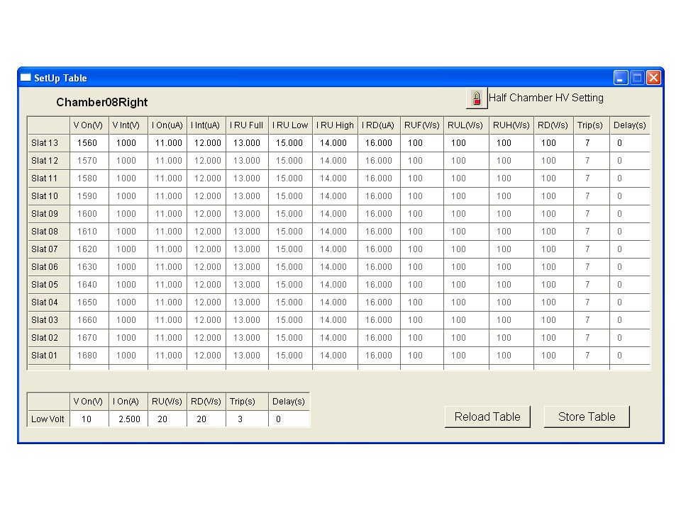
13
MCH LV for Hvd LvChm5LLvChm6l LvChm5L – Low Voltage for High Voltage Distributors on Chamber 5 Left MchHvRight MchHvLeft MchHv LvChm10L LvChn6 Chamber10L LvChn2 Chamber6L LvChn1 Chamber5L LvChm5LLvChm6lLvChm10L LvChn6 Chamber10R LvChn2 Chamber6R LvChn1 Chamber5R

14
MCH Hv Subsystem Logic Diagram – Chambers 1-4 Ch6L Ch5L Ch4L Ch3L Ch2L Ch1L Cn1L Cn6L MchHvRight Logic Unit Chamber1L Chamber2L MchHvLeft MchHv Chamber3LChamber4L Chamber1R Chamber2RChamber3RChamber4R Ch6R Ch5R Ch4R Ch3R Ch2R Ch1R Cn1R Cn6R Control Unit 3.3V 2.5V -2.5V Group1 Group4 3.3V 2.5V -2.5V Group1 Group4 HV LV

15
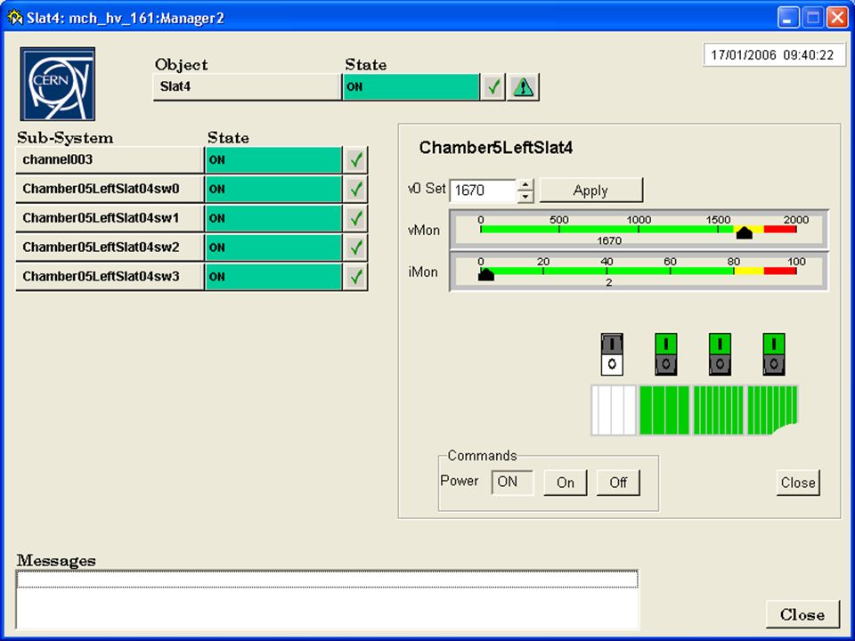
Chamber6L MchHvRight Slat1 Caen ch Chn1Hvd1Hvd2 Pcb1Pcb2 Slat9 Caen ch Chn9Hvd1Hvd2 Pcb1Pcb2 Device Unit Control Unit In Slat1, only when Chn1 is off will be possible the operation of Pcb1 and 2 via respectively Hvd1 and 2. In Slat-xx will be evaluated all the boolean conditions of the children Slat1 Caen ch Chn1Hvd1Hvd2 Pcb1Pcb2 Slat9 Caen ch Chn9 Hvd1 Hvd2 Pcb1 Pcb2 Logic Unit LV,control HV Chamber5R Chamber6R LvChm5L LvChm6R LvChn1 LvChn2 MchHvLeft MchHv Chamber5L

16
Slat1 Caen ch Chn1 Hvd1Hvd2 Pcb1 Pcb2 In Slat1L, only when Chn1 is off will be possible the operation of Pcb1 and 2 via respectively Hvd1 and 2. In Slat-xx will be evaluated all the boolean conditions of the children LvChm7L LvChn3 MchHvLeft MchHv Chamber7L Slat3 Hvd1Hvd2 Pcb1 Pcb2 Hvd3Hvd4 Pcb3 Pcb4 3.3V 2.5V-2.5V Caen ch Chn3 Slat2 Caen ch Chn2 Hvd1Hvd2 Pcb1 Pcb2 Slat4 Hvd1Hvd2 Pcb1 Pcb2 Hvd3Hvd4 Pcb3 Pcb4 Caen ch Chn4 Pcb3 Hvd2 Pcb5 Hvd5 Group1 Chamber8L

17
Slat5 Caen ch Chn5 Hvd1Hvd2 Pcb1 Pcb2 In Slat1L, only when Chn1 is off will be possible the operation of Pcb1 and 2 via respectively Hvd1 and 2. In Slat-xx will be evaluated all the boolean conditions of the children MchHvLeft MchHv Chamber7L Hvd3Hvd4 Pcb3 Pcb4 Hvd5 Pcb5 3.3V2.5V-2.5V Slat9 Hvd1Hvd2 Pcb1 Pcb2 Hvd3Hvd4 Pcb3 Pcb4 Group6 3.3V2.5V-2.5V Caen ch Chn9 Pcb4 Hvd5 Group7 Group 7 = group 1(slide before) supply slats from 10 to 13. Groups 3, 4 and 5 equals to 2 and 6 supplied slats 6, 7 and 8. Group2 Chamber8L
 supply slats from 10 to 13. Groups 3, 4 and 5 equals to 2 and 6 supplied slats 6, 7 and 8. Group2 Chamber8L.")
18
DCS COMMANDSMchHv MchHvLeft, MchHvRigt, Chamber Slat(Chn)LV (D) ChnPcb HV Power Supply A 1 OFF ONOFF B 2 3 STANDBYOFF ON C 4 DOWNLOADINGOFF ON D 5 6 STBY_CONFIGUREDOFF ONON<>OFFON ERAMP_UP_INTRAMP_UP ONON/OFFON FRAMP_UP_ONRAMP_UP ONON/OFFON G 7 8 INTERMEDIATEON ON/OFFON HDOWNLOADINGON ON/OFFON IRAMP_UP_ONRAMP_UP ONON/OFFON J 9 10 ON ON/OFFON KDOWNLOADINGON ON/OFFON LRAMP_DW_STBYRAMP_DW ONON/OFFON MRAMP_DW_INTRAMP_DW ONON/OFFON NINTERMEDIATEON ON/OFFON OSTBY_CONFIGUREDOFF ONON<>OFFON Asynchronous Events PMIXED QWA_REPAIRTRIPPED RER_REPAIR(Mj) TRIPPED S(Mj) ER_REPAIR TNO_CONTROL UWA_REPAIR VER_REPAIR WSYS_FAULT CHAN_FAULT XPWS_FAULT YINTERLOCK ZINTERLOCK_WENT Tab. 1 Summary table of states and commands for the MchHv(Left&Right), Chamber, Slat(HvChannel), Lv(Distributor), Pcb and HV Power Supply in the FSM
, Chamber, Slat(HvChannel), Lv(Distributor), Pcb and HV Power Supply in the FSM.")
19
DCS COMMANDSMchHv MchHvLeft, MchHvRigt, Chamber Slat(Chn)LV (D) ChnPcb HV Power SupplyLV GroupLV Power Supply A 1 OFF ONOFF B 2 3 STANDBYOFF ON OFFON C 4 DOWNLOADINGOFF ON OFFON D 5 6 STBY_CONFIGUREDOFF ON<>OFFONOFFON ERAMP_UP_INTRAMP_UP ONON/OFFON FRAMP_UP_ONRAMP_UP ONON/OFFON G 7 8 INTERMEDIATEON ON/OFFON HDOWNLOADINGON ON/OFFON IRAMP_UP_ONRAMP_UP ONON/OFFON J 9 10 ON ON/OFFON KDOWNLOADINGON ON/OFFON LRAMP_DW_STBYRAMP_DW ONON/OFFON MRAMP_DW_INTRAMP_DW ONON/OFFON NINTERMEDIATEON ON/OFFON OSTBY_CONFIGUREDOFF ON<>OFFONOFFON Asynchronous Events PMIXED QWA_REPAIRTRIPPED RER_REPAIR(Mj) TRIPPED S(Mj) ER_REPAIR TNO_CONTROL UWA_REPAIR VER_REPAIR WSYS_FAULT CHAN_FAULT XPWS_FAULT YINTERLOCK ZINTERLOCK_WENT Tab. 1 Summary table of states and commands for the MchHv(Left&Right), Chamber, Slat(HvChannel), Lv(Distributor), Pcb and HV Power Supply in the FSM + LV PWS and LV Group
, Chamber, Slat(HvChannel), Lv(Distributor), Pcb and HV Power Supply in the FSM + LV PWS and LV Group.")
20
DCS HV COMMANDS COMMENTS 1 GO_STANDBY or GO-OFF In STANDBY the HV power supplies are switched ON but channels OFF 2 CONFIGURE After the recipes downloading the final state is STBY_CONFIGURED 3 GO_STANDBY The user going to change states of the Pcbs(Switch OFF HV channels and ON LV) 4 CONFIGURE Useful to reconfigure the devices while in STBY_CONFIGURED 5 GO_INTERMEDIATE The HV channels are in INTERMEDIATE values 6 GO_ON Directly GO_ON from STBY_CONFIGURED 7 CONFIGURE Downloading a new configuration while in INTERMEDIATE 8 GO_ON GO_ON from INTERMEDIATE 9 GO_STBY_CONF Goes to STBY_CONFIGURED ( Switch OFF HV and LV channels) 10 GO_INTERMEDIATE Goes to INTERMEDIATE from ON Table 2. Commands from DCS DOWNLOADING RAMP_UP_INT RAMP_UP_ONRAMP_DW_INT RAMP_DW_STBY STANDBY STBY_CONFIGURED INTERMEDIATE ON OFF GO_STANDBY GO_OFF CONFIGURE(Keys) GO_STANDBY CONFIGURE(Key) GO_INTERMEDIATE GO_ON CONFIGURE(Key) GO_STBY_CONF GO_ON GO_STBY_CONF GO_INTERMEDIATE MchHv State Diagram Chamber, Slat(Channel) and LowVoltage State Diagrams OFF GO_ON ON GO_OFF NO_CONTROL TRIPPED CHAN_FAULT RECOVER Network Connection lost LV Channel State Diagram
 GO_STANDBY CONFIGURE(Key) GO_INTERMEDIATE GO_ON CONFIGURE(Key) GO_STBY_CONF GO_ON GO_STBY_CONF GO_INTERMEDIATE MchHv State Diagram Chamber, Slat(Channel) and LowVoltage State Diagrams OFF GO_ON ON GO_OFF NO_CONTROL TRIPPED CHAN_FAULT RECOVER Network Connection lost LV Channel State Diagram.")
21
OFF GO_ON Active lines on External Interlock and External Disable(SY1527) ON GO_OFF NO_CONTROL INTERLOCK_WENT INTERLOCK ERROR RECOVER RECOVER_INTERLOCK Power Crate unsafe Conditions, Kill command Network Connection lost OFF SWITCH_ON ON SWITCH_OFF NO_CONTROL Network Connection lost PWS(MchHvLeft, MchHvRight, LowVoltXX) State Diagram Pcb State Diagram A One or several tripped Channels in Chamber #trips=>Max? NoYes ER_REPAIRWA_REPAIR Go to the Appropriate state Go to the Appropriate state B NO_CONTROL From any state if the Communication with The hardware is lost When the Communication is established Go to the Appropriate state C ERROR When several modules in ER_REPAIR, or External interlock, or power crate failure, un-calibrated board Go to OFF Recovering actions Recovering actions RECOVER D INTERLOCK_WENT It is the propagation of the interlock condition in HVPS INTERLOCK Go to OFF RECOVER_INTERLOCK E MIXED From any state when not all the channels or systems are in the same state When all channels are in the same stable state Go to the Appropriate state

22
Proposal CR04-Z05-LEFT- CAEN SY 1527 Slot#0Slot#0 Slot#1Slot#1 Slot#2EmptySlot#2Empty Slot#3Slot#4Slot#5Slot#6Slot#7Slot#8Slot#9Slot#10-14 Empty 1 HV-CH5-L-1HV-CH6-L-1HV-CH7-L-1HV-CH8-L-1HV-CH9-L-1HV-CH10-L-1HV-CH7-L-13 2 HV-CH5-L-2HV-CH6-L-2HV-CH7-L-2HV-CH8-L-2HV-CH9-L-2HV-CH10-L-2HV-CH8-L-13 3 HV-CH5-L-3HV-CH6-L-3HV-CH7-L-3HV-CH8-L-3HV-CH9-L-3HV-CH10-L-3HV-CH9-L-13 4 HV-CH5-L-4HV-CH6-L-4HV-CH7-L-4HV-CH8-L-4HV-CH9-L-4HV-CH10-L-4HV-CH10-L-13 5 HV-CH5-L-5HV-CH6-L-5HV-CH7-L-5HV-CH8-L-5HV-CH9-L-5HV-CH10-L-5EMPTY 6 HV-CH5-L-6HV-CH6-L-6HV-CH7-L-6HV-CH8-L-6HV-CH9-L-6HV-CH10-L-6EMPTY 7 HV-CH5-L-7HV-CH6-L-7HV-CH7-L-7HV-CH8-L-7HV-CH9-L-7HV-CH10-L-7EMPTY 8 HV-CH5-L-8HV-CH6-L-8HV-CH7-L-8HV-CH8-L-8HV-CH9-L-8HV-CH10-L-8EMPTY 9 HV-CH5-L-9HV-CH6-L-9HV-CH7-L-9HV-CH8-L-9HV-CH9-L-9HV-CH10-L-9EMPTY 10 EMPTY HV-CH7-L-10HV-CH8-L-10HV-CH9-L-10HV-CH10-L-10EMPTY 11 EMPTY HV-CH7-L-11HV-CH8-L-11HV-CH9-L-11HV-CH10-L-11EMPTY 12 EMPTY HV-CH7-L-12HV-CH8-L-12HV-CH9-L-12HV-CH10-L-12EMPTY Used by Station 1 and 2 Used by Stations 3, 4 and 5

23
CR04-Z05-LEFT- CAEN SY 1527 ChannSlot# 0-1, 3-9 A1821P Slot# 2,10-14 Free Slot#15 A1513B 1 DLV-CH5-L-1 2 DLV-CH7-L-1 3 DLV-CH9-L-1 4 DLV-CH6-L-1 5 DLV-CH8-L-1 6 DLV-CH10-L-1 7 8 9 10 11 12 DLV-CH5-L-1 –> Distributor Low Voltage, Station 3, Chamber 5, Left, Slat 1 Proposal DLV-CH7-L-1 –> Distributor Low Voltage, Station 4, Chamber 7, Left, Slat 1 DLV-CH9-L-1 –> Distributor Low Voltage, Station 5, Chamber 9, Left, Slat 1 DLV-CH6-L-1 –> Distributor Low Voltage, Station 3, Chamber 6, Left, Slat 1 DLV-CH8-L-1 –> Distributor Low Voltage, Station 4, Chamber 8, Left, Slat 1 DLV-CH10-L-1 –> Distributor Low Voltage, Station 5, Chamber 10, Left, Slat 1

24
CR04-Z05-RIGHT- CAEN SY 1527 Slot#0Slot#0 Slot#1Slot#1 Slot#2EmptySlot#2Empty Slot#3Slot#4Slot#5Slot#6Slot#7Slot#8Slot#9Slot#10-14 Empty 1 HV-CH5-R-1HV-CH6-R-1HV-CH7-R-1HV-CH8-R-1HV-CH9-R-1HV-CH10-R-1HV-CH7-R-13 2 HV-CH5-R-2HV-CH6-R-2HV-CH7-R-2HV-CH8-R-2HV-CH9-R-2HV-CH10-R-2HV-CH8-R-13 3 HV-CH5-R-3HV-CH6-R-3HV-CH7-R-3HV-CH8-R-3HV-CH9-R-3HV-CH10-R-3HV-CH9-R-13 4 HV-CH5-R-4HV-CH6-R-4HV-CH7-R-4HV-CH8-R-4HV-CH9-R-4HV-CH10-R-4HV-CH10-R-13 5 HV-CH5-R-5HV-CH6-R-5HV-CH7-R-5HV-CH8-R-5HV-CH9-R-5HV-CH10-R-5EMPTY 6 HV-CH5-R-6HV-CH6-R-6HV-CH7-R-6HV-CH8-R-6HV-CH9-R-6HV-CH10-R-6EMPTY 7 HV-CH5-R-7HV-CH6-R-7HV-CH7-R-7HV-CH8-R-7HV-CH9-R-7HV-CH10-R-7EMPTY 8 HV-CH5-R-8HV-CH6-R-8HV-CH7-R-8HV-CH8-R-8HV-CH9-R-8HV-CH10-R-8EMPTY 9 HV-CH5-R-9HV-CH6-R-9HV-CH7-R-9HV-CH8-R-9HV-CH9-R-9HV-CH10-R-9EMPTY 10 EMPTY HV-CH7-R-10HV-CH8-R-10HV-CH9-R-10HV-CH10-R-10EMPTY 11 EMPTY HV-CH7-R-11HV-CH8-R-11HV-CH9-R-11HV-CH10-R-11EMPTY 12 EMPTY HV-CH7-R-12HV-CH8-R-12HV-CH9-R-12HV-CH10-R-12EMPTY Proposal Used by Station 1 and 2 Used by Stations 3, 4 and 5

25
CR04-Z05-RIGHT- CAEN SY 1527 ChannSlot# 0-1,3-9 A1821P Slot# 2,10-14 Free Slot#15 A1513B 1 DLV-CH5-R-1 2 DLV-CH7-R-1 3 DLV-CH9-R-1 4 DLV-CH6-R-1 5 DLV-CH8-R-1 6 DLV-CH10-R-1 7 8 9 10 11 12 DLV-CH5-R-1 –> Distributor Low Voltage, Station 3, Chamber 5, Right, Slat 1 Proposal DLV-CH7-R-1 –> Distributor Low Voltage, Station 4, Chamber 7, Right, Slat 1 DLV-CH9-R-1 –> Distributor Low Voltage, Station 5, Chamber 9, Right, Slat 1 DLV-CH6-R-1 –> Distributor Low Voltage, Station 3, Chamber 6, Right, Slat 1 DLV-CH8-R-1 –> Distributor Low Voltage, Station 4, Chamber 8, Right, Slat 1 DLV-CH10-R-1 –> Distributor Low Voltage, Station 5, Chamber 10, Right, Slat 1

31
Planning for installation of Muon Tracking Chambers in the PIT No:Task NameStartFinishDuration 1Install Tracking station 4-CH7Thu 06/08/06Wed 07/19/066 week 2Install Tracking station 4-CH8Tue 06/20/06Mon 07/31/0630 days 3Install Tracking station 5-CH9Tue 08/15/06Mon 09/25/0630 days 4Install Tracking station 5-CH10Wed 10/11/06Tue 11/21/0630 days 5Install Tracking station 3-CH5Wed 12/06/06Tue 01/16/0730 days 6Install Tracking station 4-CH6Wed 02/14/07Tue 03/27/0730 days 7Install Tracking station 1Mon 06/19/06Fri 12/29/0628 weeks 8Install Tracking station 2Mon 06/19/06Fri 12/29/0628 weeks

Similar presentations


 Iseg OPC server HV Iseg crates (3)LV Wiener crates (22) CAN bus Interface to FEE -temp.mon -I &V mon. Wiener OPC server.>")

 Serguei Sadovsky (IHEP, Protvino) CERN, DCS meeting, 30 January, 2007.>")

 on behalf of WP 8.5.3 group Gif++ User Meeting 11/07/2014 Outline Status.>")

 TDR 28 January 2004 L.Jirdén On behalf of ALICE Controls Coordination (ACC): A.Augustinus, P.Chochula, G. De Cataldo,>")


