Download presentation
Presentation is loading. Please wait.

1
Synchronous logical networks II
Digital Systems M

2
Decoder Counter The value of base 4 counter CB2CLED is decoded and triggers a variation of FF1 (which selects the counter direction)) when 0 is reached if Down (3 if Up). The signal enabling the FF switch acting on the three ways MUX, inverted, is also the counter enable. Therefore when the counter direction inversion is enabled the counter is disabled
) when 0 is reached if Down (3 if Up). The signal enabling the FF switch acting on the three ways MUX, inverted, is also the counter enable. Therefore when the counter direction inversion is enabled the counter is disabled.")
3
Behavioural simulation

4
A retriggerable one-shot (trigger => activation signal) is circuit which generates a Z output pulse lasting T (T presettable) after a positive edge of an input signal X. When another positive edge of X occurs during the pulse Z, the circuit extends the pulse Z of another T time. Design a synchronous retriggerable one-shot (Moore) which using an input signal X asynchronous to a clock (of frequency f=1/T) produces in a retriggerable way a pulse of 5T, synchronous with the clock. Direct synthesis 3 Normal one-shot Retriggerable one-shot

5
A type monoimpulsor After the RESET and until a «1» occurs on X (trigger), the circuit output is 0 (the Reset acts on the output FF CLR). When X=1 the monoimpulsor sends a ‘1’ to the output FF which swtches to 1 at the next clock positive edge (and keeps 1 because of the feedback OR) and at the same time resets and activates the counter (CLR asynchronous and counter CE = ‘1’), which will be active until the counter reaches 5 zeroing the circuit output. In case of a further input trigger the output FF remains 1 and the counter is Reset (retrigger effect)
, the circuit output is 0 (the Reset acts on the output FF CLR). When X=1 the monoimpulsor sends a ‘1’ to the output FF which swtches to 1 at the next clock positive edge (and keeps 1 because of the feedback OR) and at the same time resets and activates the counter (CLR asynchronous and counter CE = ‘1’), which will be active until the counter reaches 5 zeroing the circuit output. In case of a further input trigger the output FF remains 1 and the counter is Reset (retrigger effect)")
6
Behavioural Simulation
Retrigger Non sampled input Reset 5 periods Post-Route Simulation The simulation activates first a reset signal to reset the circuit state then after two clock periods two successive «1» inputs delayed of two periods are sent to the input. It can ve verified that the output remains 1 for (2+5) clock periods. The second part of the simulations deals with a not detected too short trigger. In the last part it is verified that the if the input is kept constant 1 the circuits doesn’t retrigger (a zero input must be inserted)
 clock periods. The second part of the simulations deals with a not detected too short trigger. In the last part it is verified that the if the input is kept constant 1 the circuits doesn’t retrigger (a zero input must be inserted)")
7
Waveforms generation Q Clock 3T 3T 2T Z Z T Clock Cx5
It is possbile to generate periodical waveforms through synchronous circuits whose period is an integer submultiple of che clock period Q D0..k Q0..k CK D !Q Example 1: by 2 frequency divider Clock Example 2: generation of a waveform with 5T period (T period of the clock) whose output is high for 3T and low for 2T Cx5 CK Q0 Q1 Q2 3T 3T 2T Z C B A 1 2 3 4 Z T Clock Decoder/Demux (NB: if the outputs were negative true a NAND instead of the OR should be used NB: a logical network can only implement frequency dividers and never frequency multipliers (which can be achieved only through non linear analog circuits)
 whose output is high for 3T and low for 2T. Cx5. CK. Q0 Q1 Q2. 3T. 3T. 2T. Z. C. B. A Z. T. Clock. Decoder/Demux (NB: if the outputs were negative true a NAND instead of the OR should be used. NB: a logical network can only implement frequency dividers and never frequency multipliers (which can be achieved only through non linear analog circuits)")
8
What sort of circuit is this ?
D0..k Q0..k CK D0 !Q0 D1 !Q1 D2 !Q2 Clock NB: The clock signal is not the same for all FFs (7493) Clock !Q0 !Q1 !Q2 This is not a synchronous binary counter (it is called also an asynchronous counter). Its FFs do not use the same clock signal and this implies that among the FFs outputs a little disalignment takes place. This sort of circuit can’t be synthesized as a synchronous circuit and a formal synthesis can be achieved only by considering the circuit as asynchronous that is by “opening” the FFs. (How many states in this case ?)
 Clock. !Q0. !Q1. !Q2. This is not a synchronous binary counter (it is called also an asynchronous counter). Its FFs do not use the same clock signal and this implies that among the FFs outputs a little disalignment takes place. This sort of circuit can’t be synthesized as a synchronous circuit and a formal synthesis can be achieved only by considering the circuit as asynchronous that is by opening the FFs. (How many states in this case )")
9
Xilinx asynchronous counter

10
How can a DFF catch a pulse shorter than a clock period ?
Type A monoimpulsor “revisited” D2 Q2 !Q2 CK DFF Z Clock D1 Q1 !Q1 D0 Q0 !Q0 “1” CL Ths short pulse is «captured» by FF 0 (provided it is sufficiently wide for the FF technology) – which acts as an integrator – whose output is fed to the A type monoimpulsor. The output of FF1 resets the FF0 (if CL is “positive”true”). Can a problem arise since the Clear is asynchronous? NB:This circuits and the previous one underline the fact no network is intrinsically synchronous and that in general it is almost always necessary the use of circuits of different nature. This is in any case true because there are always interacting networks which use different clocks and input signals not synchronous
 – which acts as an integrator – whose output is fed to the A type monoimpulsor. The output of FF1 resets the FF0 (if CL is positive true ). Can a problem arise since the Clear is asynchronous NB:This circuits and the previous one underline the fact no network is intrinsically synchronous and that in general it is almost always necessary the use of circuits of different nature. This is in any case true because there are always interacting networks which use different clocks and input signals not synchronous.")
11
Shift registers A left (right) shift register is a register made of DFFs, which at each clock positive edge copies the value of its right ((left) FF. In the last FF on the right (left ) a “0” is copied. This type of shift register is called «logic shift register». “0” D0..k Q0..k CK Dn Qn D0..k Q0..k CK Dn-1 Qn-1 D0..k Q0..k CK Dn-2 Qn-2 D0..k Q0..k CK D0 Q0 Left shift register For the shift registers too there are many versions: parallel in serial output, serial input parallel output, with or without reset, load signals etc. etc. A shift register is also a counter. If upon a reset the input of FF0 is kept to 1 the shift register is incrementally filled with «1»: the number of «1» (or the position of the leftmost 1) indicates the count value Very often the same register can shift either left or right according to an input control signal. This is achieved inserting a 2-way Mux before each D input, whose inputs are the outputs of either the left or right FF (Qì+1 or Qì-1.). With this configuration the shift register becomes an Up/down counter
 shift register is a register made of DFFs, which at each clock positive edge copies the value of its right ((left) FF. In the last FF on the right (left ) a 0 is copied. This type of shift register is called «logic shift register». 0 D0..k. Q0..k. CK. Dn. Qn. D0..k. Q0..k. CK. Dn-1. Qn-1. D0..k. Q0..k. CK. Dn-2. Qn-2. D0..k. Q0..k. CK. D0. Q0. Left shift register. For the shift registers too there are many versions: parallel in serial output, serial input parallel output, with or without reset, load signals etc. etc. A shift register is also a counter. If upon a reset the input of FF0 is kept to 1 the shift register is incrementally filled with «1»: the number of «1» (or the position of the leftmost 1) indicates the count value. Very often the same register can shift either left or right according to an input control signal. This is achieved inserting a 2-way Mux before each D input, whose inputs are the outputs of either the left or right FF (Qì+1 or Qì-1.). With this configuration the shift register becomes an Up/down counter.")
12
3-bit shift-register OUT0 OUT1 OUT2 DFF DFF DFF IN D Q D Q D Q Q* Q*
A_RESET* A_RESET* A_RESET* CK

13
CK IN A_RESET OUT2 OUT1 OUT0
3-bit shift-register CK IN A_RESET OUT2 OUT1 OUT0

14
Example: 74164 (serial IN-parallel OUT)
In this shift register, for each positive clock edge (CP) data are shifted one position right (Q0 -> Q1, Q1->Q2 etc). The register has a Master Reset (MR – negative true) and the bit inserted in Q0 FF is the AND of the two inputs Dsa e Dsb It must be noticed that the shift operation corresponds arithmetically (without sign) to the division and multiplication by 2. Suppose that in Q0 the MSbit is stored and in Q7 the LSbit Shift left => x2 = 21210 Q7 Q6 Q5 Q4 Q3 Q2 Q1 Q0 L/R CK = 10610 Shift right => /2 = 5310 Weight
 data are shifted one position right (Q0 -> Q1, Q1->Q2 etc). The register has a Master Reset (MR – negative true) and the bit inserted in Q0 FF is the AND of the two inputs Dsa e Dsb. It must be noticed that the shift operation corresponds arithmetically (without sign) to the division and multiplication by 2. Suppose that in Q0 the MSbit is stored and in Q7 the LSbit. Shift left => x = Q7 Q6 Q5 Q4 Q3 Q2 Q1 Q0. L/R. CK = Shift right => / = Weight")
15
11100101 interpreted as 2’s complement
Arithmetic Shift There are also arithmetic shift registers. In these right shift registers instead of inserting a “0” in the most left FF the same logic value is always inserted Q7 Q6 Q5 Q4 Q3 Q2 Q1 Q0 D7 D6 D5 D4 D3 D2 D1 D0 I LD CK Example Arithmetic Shift Right interpreted as 2’s complement negative numbers Shifting right C2 C2 = 5410 = 2710 The arithmetic right shift implements a division by 2 maintaining the sign !! Obviously the same holds for the positive numbers.

16
Rotation In the computers it is often necessary to implement a right or left rotation of a register content. This is achieved by a feedback shift register D0..k Q0..k CK Dn Qn D0..k Q0..k CK Dn-1 Qn-1 D0..k Q0..k CK Dn-2 Qn-2 D0..k Q0..k CK D0 Q0 Very often the direction must be programmable In this case the input of D0 (through a MUX 2:1) can be Q1 or Qnand so on
 can be Q1 or Qnand so on.")
17
Shift register counters
Shift register based counter through EX-OR feedback 3 bit shift right D Q0 Q1 Q2 100 110 111 011 101 010 001 000 Disjoint state diagram !! A n FF shift register with an EX-OR feedback (with variable inputs selected) is a NON binary counter for 2n-1 (provided it is not preset with all zeros)
 is a NON binary counter for 2n-1 (provided it is not preset with all zeros)")
18
Disjoint state loop : 101->010->101..>1
Johnson Counter FFD D Q Q* R* A_RESET* OUT2 OUT1 OUT0 CK 000->100->110->111->011->001->000->.. . Disjoint state loop : 101->010->101..>1 A Johnson counter with N FFs counts for 2N. Since successive Johnson counter configurations differ by a single bit (adjacent configurations) it can be used for generating glitches-free waveforms
 it can be used for generating glitches-free waveforms.")
19
0001->1000->0100->0010->0010
Single «1» ring counter (directly generating a 1 over n code) OUT0 OUT1 OUT2 OUT3 FFD FFD FFD FFD D Q D Q D Q D Q Q* Q* Q* Q* R* R* R* PR* RESET* RESET* RESET* RESET* CK 0001->1000->0100->0010->0010 The ring counter needs N FFs in order to count for N (while with the binary counters the number of FF necessary for a N count is m= |log2N| that is the first integer greater or equal to log2N)
 OUT0. OUT1. OUT2. OUT3. FFD. FFD. FFD. FFD. D. Q. D. Q. D. Q. D. Q. Q* Q* Q* Q* R* R* R* PR* RESET* RESET* RESET* RESET* CK >1000->0100->0010->0010. The ring counter needs N FFs in order to count for N (while with the binary counters the number of FF necessary for a N count is m= |log2N| that is the first integer greater or equal to log2N)")
20
Synchronous networks exercises presented in the course are based on the state diagram but only for verification! Synchronous network synthesis is made WITHOUT the state diagram using….. the brain only by decomposing the network in well know blocks (FFs, combinatorial networks and – see later – counters, shift registers etc.etc.)…
….")
21
RSS D P Enable V Exercise 4 synchronous E
Design a synchronous logical network (SRL) able to detect palindrome 4 bit configurations (that is configurations that are identical when read left to right or viceversa) which are sequentially inserted in a shift register. The D input is significant (and therefore valid for the sequence) only when the input Enable is 1 (whichs is not necessarilly the case for four consecutive input bits). The output P is 1 for a single period when a palindrome configuration is detected after a 4 bit sequence is received. Then a new 4 bit sequence must be received (by E conditioned) and detected. Direct synthesis RSS D V P Enable E Exercise 4 synchronous
 able to detect palindrome 4 bit configurations (that is configurations that are identical when read left to right or viceversa) which are sequentially inserted in a shift register. The D input is significant (and therefore valid for the sequence) only when the input Enable is 1 (whichs is not necessarilly the case for four consecutive input bits). The output P is 1 for a single period when a palindrome configuration is detected after a 4 bit sequence is received. Then a new 4 bit sequence must be received (by E conditioned) and detected. Direct synthesis. RSS. D. V. P. Enable. E. Exercise 4 synchronous.")
22
To store a 4 bit sequence a Shift Register with Enable (CE) and Clear (CLR) is used. A palindrome configuration is detected when the 1st bit is equal to the 4th bit and the 2nd bit is equal to the 3rd bit .

23
A by 4 counter is used: upon the 4th clock positive edge the network controls whether the configuration is palindrome. The DFF after the decoding of 3 (that is when the counter becomes 0 anew) is used because the configuration control must be delayed un period. The ENABLE signal is connected to both components (when 0 both the counter and the shift are disabled). NB: The first inserted bit is sampled when the counter is increased from 0 to 1 NB: in this circuit Preset and Clear signals are not connected. In Xilinx unconnected control signals are inactive

24
POST-ROUTE SIMULATION
Z output is delayed 10 ns from the clock positive edge because of the switch delay Not valid input Enable=0

25
Barrel shifter (rotor)
A barrel shifter is a shift register able to shift “n” positions in a single period its FFs contents. A-H inputs are synchronously stored in the FFs when the LDST is activated. When LDST is 0 upon each clock positive edge an anticlockwise n-positions rotation takes place where n is the binary value of S0, S1 and S2 signals. For instance if ” ” is rotated 4 positions at the first clock the content becomes “ ”. If then it is rotated 3 positions it becomes “ ” It must be noticed that the component is a register with «n» 8:1 Muxs, each one connected to the D inputs of the FFs. The Mux control input value n is given by S0, S1 and S2.

26
Xilinx schematic The last six right signals are the true and inverted selection signals (S1, !S1, S2, !S2, S3 e !S3) for the 8:1 MUXs Preset value The circuit in figure is one of the eight 8:1 MUXs which select the values to be stored in the FFs MUX The first left 8 signals are the values of the FF D inputs in the preceding period Each 8:1 MUX is ORed with preset input value which is used together with !LOAD (if LOAD=1 the OR preset value is 0). The FF output is ANDed with !LOAD: this zeroes all MUX outputs allowing the preset values to be stored in the FFs
. The FF output is ANDed with !LOAD: this zeroes all MUX outputs allowing the preset values to be stored in the FFs.")
27
LDST=LOAD Si -> Mux 8:1 control signal of each FF
A..H -> segnals for Preset /Load Preset AND LDST=LOAD When LDST signal is 0 all preset ANDs are zero. If LDST is 1 the preset signals are enabled and all MUX outputs are zeroed

28
First 4 FFs Preset values.
The LOAD (LDST) signal enables the preset inputs of the FFs (see the ANDs of the previous figure) and at the same time zeroes the output of the FFs (see the FFs cascaded ANDs) so as to select the preset value of the OR input
 signal enables the preset inputs of the FFs (see the ANDs of the previous figure) and at the same time zeroes the output of the FFs (see the FFs cascaded ANDs) so as to select the preset value of the OR input.")
29
Xilinx schematic S2, S1, S0 selection signals QA, QB, QC, ..., QH
Outputs signals A, B, C, ..., H Input signals LDST load signal Clock

30
This new value can be rotated again
Barrel Shifter LDST=1:upont the first clock positive edge the “ ” value is loaded into the Barrel Shifter. A further active LDST loads a new valute into the the Barrel Shifter. This new value can be rotated again according to S signals The different values of Si (1, 3, 5) cause different device rotation, Obviously with 8 sigle shifts the value becomes the initial value “ ” again This is a typical example of how erroneous is not to «bus» signals a-g, qa-g and S0-2. It would have been possible to use a compact decomposable binary notation much easier to interpret, where all single signals can be however displayed by «opening» the bus
 cause different device rotation, Obviously with 8 sigle shifts the value becomes the initial value again. This is a typical example of how erroneous is not to «bus» signals a-g, qa-g and S0-2. It would have been possible to use a compact decomposable binary notation much easier to interpret, where all single signals can be however displayed by «opening» the bus.")
31
EPROM based synchronous networks
Z0..m X0..n EPROM Y0..k y0..k D0..k D0..k Q0..k Q0..k CK CK Clock FFD0..k Nowadays instead of the EPROMs PLAs (Programmable Logical Arrays) are used, that is devices where the combinatorial functions are optimized (combinatorial functions implementations are not necessarily canonical). The basic principle is however the same.
 are used, that is devices where the combinatorial functions are optimized (combinatorial functions implementations are not necessarily canonical). The basic principle is however the same.")
32
This is the basic architecture of the central unit of any computer
Exercise Design with Xilinx a synchronous logical network using 374, ALU 74181, a counter and other necessary devices which implements in sequence (after a START) signal the sum of two four bits absolute numbers (A and B) then 2’s complements the result, then exchanges the two MSBits with the two LSBits and eventually divides arythmetically the result by 2. Example A=1100 B=0101 => Sum 0001 Exchange => 0100 (410) 2’s complement => 1100 (-410) Arithmetical division (right shift) by two => 1110 (-210) The solution can be decomposed in three subsystems: the control and decoding unit, the datapath, the input and output registersi. This is the basic architecture of the central unit of any computer The only difference is that for the computers instead of a fixed sequence of elementary operations a new different sequence is generated for each instruction which must be executed.
 signal the sum of two four bits absolute numbers (A and B) then 2’s complements the result, then exchanges the two MSBits with the two LSBits and eventually divides arythmetically the result by 2. Example. A=1100 B=0101 => Sum Exchange => 0100 (410) 2’s complement => 1100 (-410) Arithmetical division (right shift) by two => 1110 (-210) The solution can be decomposed in three subsystems: the control and decoding unit, the datapath, the input and output registersi. This is the basic architecture of the central unit of any computer. The only difference is that for the computers instead of a fixed sequence of elementary operations a new different sequence is generated for each instruction which must be executed.")
33
Exercise The synchronous network of figure must add modulo 256 the 8 bit data received in parallel on lines D[7..0]. The sum must be updated each clock and presented on the output lines OUT[7..0]. In case the input data is 68H the sum must not be updated and the input data discarded. In addition whenever 6 significant data have been received (that is excluding 68H) the output signal F must be set for one clock period during the reception of the sixth data. A reset input is also available which zeroes the outputs and resets the data count. Direct design RSS A_RES D[7..0] OUT[7..0] F Clock
 the output signal F must be set for one clock period during the reception of the sixth data. A reset input is also available which zeroes the outputs and resets the data count. Direct design. RSS. A_RES. D[7..0] OUT[7..0] F. Clock.")
34
RSS D[7..0] OUT[7..0] DEC_68 signal synthesis DEC(68h) D[7..0] DEC_68
A_RES RSS D[7..0] OUT[7..0] A_RES F RSS A_RES D[7..0] D[7..0] OUT[7..0] OUT[7..0] F CLK DEC_68 signal synthesis DEC(68h) D[7..0] DEC_68
![RSS D[7..0] OUT[7..0] DEC_68 signal synthesis DEC(68h) D[7..0] DEC_68](http://slideplayer.com/slide/3249294/11/images/34/RSS+D%5B7..0%5D+OUT%5B7..0%5D+DEC_68+signal+synthesis+DEC%2868h%29+D%5B7..0%5D+DEC_68.jpg "A_RES. RSS. D[7..0] OUT[7..0] A_RES. F. RSS. A_RES. D[7..0] D[7..0] OUT[7..0] OUT[7..0] F. CLK. DEC_68 signal synthesis. DEC(68h) D[7..0] DEC_68.")
35
374 Modulo 256 adder Full Adder 8 bit OUT[7..0] D[7..0] DEC_68 1 A_RES
Q* Q CLK 1 DEC_68 OE OUT[7..0] CIN A[7..0] B[7..0]
![374 Modulo 256 adder Full Adder 8 bit OUT[7..0] D[7..0] DEC_68 1 A_RES](http://slideplayer.com/slide/3249294/11/images/35/374+Modulo+256+adder+Full+Adder+8+bit+OUT%5B7..0%5D+D%5B7..0%5D+DEC_68+1+A_RES.jpg "Q* Q. CLK. 1. DEC_68. OE. OUT[7..0] CIN. A[7..0] B[7..0]")
36
8 bit counter F signal synthesis DEC(5h) Synchronous RESET DEC_68* F
A_RES 8 bit counter A_RES DEC_68* EN F RES CLK U2 U1 U0 DEC(5h) F
 F.")
37
Exercise A synchronous sequential network must monitor the data received on the 8 lines D[7..0]: the data received are significant only if N=1. The networks must count modulo 256 how many data are divisible by 4 while EN=1 (excluding 0). The network has two more inputs THREE e RESET. The signal THREE when asserted indicates that the value for increasing the count (if the data is divisible by 4) must be 3 (on the contrary if THREE is 0 the count must be increased by 1). The synchronous RESET signal overrides all other signals. Direct design.
. The network has two more inputs THREE e RESET. The signal THREE when asserted indicates that the value for increasing the count (if the data is divisible by 4) must be 3 (on the contrary if THREE is 0 the count must be increased by 1). The synchronous RESET signal overrides all other signals. Direct design.")
38
An 8 integrated bit register is used for the solution.
Synchronous Sequential Network I[7..0] I[7..0] U[7..0] U[7..0] (Count) EN EN THREE THREE RESET RESET CK An input data is divisible by 4 of its two Lsbits (I1 and I0) are zero. An 8 integrated bit register is used for the solution.
 EN. EN. THREE. THREE. RESET. RESET. CK. An input data is divisible by 4 of its two Lsbits (I1 and I0) are zero. An 8 integrated bit register is used for the solution.")
39
DEC(0) Signal DEC(0) is 1 if all input bits are 0 I[7..0] DEC(0)
A signal DIV4 decodes whether the input data is divisible by 4 and NOT zero: DIV4 = !I1·!I0·!DEC(0) A signal STORE indicates that EN=1 and the input datum is divisible by 4: STORE = EN·DIV4
![DEC(0) Signal DEC(0) is 1 if all input bits are 0 I[7..0] DEC(0)](http://slideplayer.com/slide/3249294/11/images/39/DEC%280%29+Signal+DEC%280%29+is+1+if+all+input+bits+are+0+I%5B7..0%5D+DEC%280%29.jpg "A signal DIV4 decodes whether the input data is divisible by 4 and NOT zero: DIV4 = !I1·!I0·!DEC(0) A signal STORE indicates that EN=1 and the input datum is divisible by 4: STORE = EN·DIV4.")
40
REG 8 BIT FA 8 bit STORE + RESET EN ‘0’ 1 D[7..0] Z[7..0] U[7..0]
RESET 8 Mux 2:1 CK FA 8 bit Cout Cin ‘0’ S[7..0] A[7..0] 1 ‘3’ B[7..0] ‘1’ The FA adds 1 or 3 according to signal THREE (provided the input datum is divisble by 4 and is not 0) THREE
![REG 8 BIT FA 8 bit STORE + RESET EN ‘0’ 1 D[7..0] Z[7..0] U[7..0]](http://slideplayer.com/slide/3249294/11/images/40/REG+8+BIT+FA+8+bit+STORE+%2B+RESET+EN+%E2%80%980%E2%80%99+1+D%5B7..0%5D+Z%5B7..0%5D+U%5B7..0%5D.jpg "RESET. 8 Mux. 2:1. CK. FA 8 bit. Cout. Cin. ‘0’ S[7..0] A[7..0] 1. ‘3’ B[7..0] ‘1’ The FA adds 1 or 3 according to signal THREE (provided the input datum is divisble by 4 and is not 0) THREE.")
41
Exercise Design a synchronous sequential network which according to two programming bits X1 and X0 generates the following four output sequences of two bits (signals U1 and U0) which end always with 11: if X1=0 e X0=0 if X1=0 e X0=1 if X1=1 e X0=0 if X1=1 e X0=1 The programming signals X1 and X0 are significant only when the output is 11. The network has an synchronous RESET. Direct synthesis RSS CK X1 X0 U1 U0
 which end always with 11: if X1=0 e X0= if X1=0 e X0= if X1=1 e X0= if X1=1 e X0=1. The programming signals X1 and X0 are significant only when the output is 11. The network has an synchronous RESET. Direct synthesis. RSS. CK. X1. X0. U1. U0.")
42
The counter must be reset when U1U0 = 11
RSS CK X1 X0 U1 U0 The SSN uses a modulo N counter with N coded by the two input signals X1 e X0 (sampled when U1U0=11). if X1=0 and X0=0 ⇒ modulo 5 if X1=0 and X0=1 ⇒ modulo 7 if X1=1 and X0=0 ⇒ modulo 4 if X1=1 and X0=1 ⇒ modulo 6 For the solution we can use a module 8 counter with synchronous RES and a combinatorial network with X1 and X0 as inputs. Since the signals X1 and X0 are significant only when U1U0 = 1 they must be sampled (X1_C e X0_C) through two flip-flops when the SSN output is U1U0 = 11. .The signals U1 and U0 are the decoding of the module 8 counter status according to X1_C and X0_C. The counter must be reset when U1U0 = 11
 if X1=0 and X0=0 ⇒ modulo if X1=0 and X0=1 ⇒ modulo if X1=1 and X0=0 ⇒ modulo if X1=1 and X0=1 ⇒ modulo 6. For the solution we can use a module 8 counter with synchronous RES and a combinatorial network with X1 and X0 as inputs. Since the signals X1 and X0 are significant only when U1U0 = 1 they must be sampled (X1_C e X0_C) through two flip-flops when the SSN output is U1U0 = 11. .The signals U1 and U0 are the decoding of the module 8 counter status according to X1_C and X0_C. The counter must be reset when U1U0 = 11.")
43
D D X1_S e X0_S synthesis X1_S X1 X0_S X0 DEC(U1=1,U0=1)
D OE D Q X1_S X1 1 CK Q* A_RES DEC(U1=1,U0=1) A_RES 1 D OE D Q X0_S X0 1 CK Q* A_RES DEC(U1=1,U0=1) A_RES
 A_RES. 1. D. OE. D. Q. X0_S. X0. 1. CK. Q* A_RES. DEC(U1=1,U0=1) A_RES.")
44
10-01-01 -10 -11 if X1=0 and X0=0 ⇒ modulo 5 (0 to 4…)
U1 and U0 truth table if X1=0 and X0=0 ⇒ modulo (0 to 4…) if X1=0 and X0=1 ⇒ modulo 7 if X1=1 and X0=0 ⇒ modulo 4 if X1=1 and X0=1 ⇒ modulo 6 X1_S and X0_S values Cont. | 000 | 001, , , ,01 001 | 010, , , ,10 010 | 011, , , ,10 011 | 011, , , ,10 | 000, , ,10 101 | , ,11 110 | , | Status, U1U0 Is this synthesis of the network safe? No, beacuse the don’t cares could keep the network stable out of the main cycles
 if X1=0 and X0=1 ⇒ modulo if X1=1 and X0=0 ⇒ modulo if X1=1 and X0=1 ⇒ modulo 6. X1_S and X0_S values. Cont. | | 001,10 001,10 001,00 001, | 010,01 010,01 010,10 010, | 011,01 011,10 011,00 011, | 011,10 100,01 000,11 100,10. | 000,11 101, , | , , | , | Status, U1U0. Is this synthesis of the network safe No, beacuse the don’t cares could keep the network stable out of the main cycles.")
45
Exercise Design (direct design) a SSN which ininterruptedly checks and counts, according to the subsequently explained rules, whether the last 4 bits received on a serial input IN are either “1001” or “0110”. Whenever the “1001” is received, a module 16 counter must be incremented by 1, on the contrary if the sequence “0110”is received the counter must be decreased by 1. Upon all other sequences the counter status doesn’t change. If the counter status is no decrement in any case can take place. If the counter status is 1111 it must be incremented if the right sequence (“1001”) is received . Design the combinatorial networks RC1 and RC2 which allows to check whether the last 4 received bits (B3, B2, B1, B) are “1001” or “0110”. Design a module 16 counter (up-down) with U/!D and EN inputs using module 4 up/down counters with U/!D and EN. The system must have an output Z signalling the overflow or the attempted underflow of the counter RC1 B3 B2 B1 B0 RC2 Z1=1 if “1001” Z2=1 if “0110”
 a SSN which ininterruptedly checks and counts, according to the subsequently explained rules, whether the last 4 bits received on a serial input IN are either 1001 or Whenever the 1001 is received, a module 16 counter must be incremented by 1, on the contrary if the sequence 0110 is received the counter must be decreased by 1. Upon all other sequences the counter status doesn’t change. If the counter status is 0000 no decrement in any case can take place. If the counter status is 1111 it must be incremented if the right sequence ( 1001 ) is received. . Design the combinatorial networks RC1 and RC2 which allows to check whether the last 4 received bits (B3, B2, B1, B) are 1001 or Design a module 16 counter (up-down) with U/!D and EN inputs using module 4 up/down counters with U/!D and EN. The system must have an output Z signalling the overflow or the attempted underflow of the counter. RC1. B3. B2. B1. B0. RC2. Z1=1 if 1001 Z2=1 if 0110")
46
Question 1 Question 2 Counter X4
Design the combinatorial networks RC1 and RC2 which allows to check whether the last 4 received bits (B3, B2, B1, B) are “1001” or “0110”. Z1 = B3 !B2 !B1 B0 (1001) Z2 = !B3 B2 B1 !B0 (0110) Question 2 Design a module 16 counter (up-down) with U/!D and EN inputs using module 4 up/down counters with U/!D and EN. U/!D Counter X4 EN U0 U1 TC CK Z U3 U2 NB: TC=1 when U1=U0=1 if UP or when U1=U0=0 if Down
 are 1001 or Z1 = B3 !B2 !B1 B0 (1001) Z2 = !B3 B2 B1 !B0 (0110) Question 2. Design a module 16 counter (up-down) with U/!D and EN inputs using module 4 up/down counters with U/!D and EN. U/!D. Counter X4. EN. U0. U1. TC. CK. Z. U3. U2. NB: TC=1 when U1=U0=1 if UP or when U1=U0=0 if Down.")
47
Question 3 4 bit SHIFT REGISTER
IN IN CK S3 S2 S1 S0 B3 B2 B1 B0 RC1 IN B2 B1 B0 RC2 Z1=1 if “1001” Z2=1 if “0110”

48
Counter X16 EN U0 U1 Z U2 U3 U/!D Z1 CK S0 S1 S2 S3 ENABLE
The counter is always enabled if the received sequence is “1001” (Z1=1),and disabled when the sequence “0110” (Z2=1) is received AND at the same time the counter status 0000 with DOWN enabled (!Z=1) Z1 = B3·!B2·!B1· B0 (1001) (command Up > U/!D=1) Z2 = !(!B3· B2· B1·!B0) (0110) (command Down –> U/!D=0) ENABLE = Z1 + !Z2·!Z0 (Z0 is «0000» decoded) NB if ENABLE=0 U/!D has no meaning Z = DEC(“1111”)·(U/!D)+ DEC(“0000”)·!(U/!D)
,and disabled when the sequence 0110 (Z2=1) is received AND at the same time the counter status 0000 with DOWN enabled (!Z=1) Z1 = B3·!B2·!B1· B0 (1001) (command Up -> U/!D=1) Z2 = !(!B3· B2· B1·!B0) (0110) (command Down –> U/!D=0) ENABLE = Z1 + !Z2·!Z0 (Z0 is «0000» decoded) NB if ENABLE=0 U/!D has no meaning. Z = DEC( 1111 )·(U/!D)+ DEC( 0000 )·!(U/!D)")
49
Exercise Synchronous network
Design a periodic rectangular waveform generator (T=5ns – frequency ?) with programmable duty-cycle (the percentage of a period where the signal is 11). The duty cycle is coded by two input signals I1 e I0 as follows: I1I0 = 00 duty-cycle 10% I1I0 = 01 duty-cycle 30% I1I0 = 10 duty-cycle 50% I1I0 = 11 duty-cycle 80% I1 and I0 are meaningful only if the input signal SET is 1: in this case a new duty cycle is set starting from the next clock. The clock period is 500ps (frequency ?) . The system is based on a modulo 16 counter with ENABLE and synchronous RESET. 10% 30% 50% 80% SET Synchronous network I1 Z I0 CK
 with programmable duty-cycle (the percentage of a period where the signal is 11). The duty cycle is coded by two input signals I1 e I0 as follows: I1I0 = 00 duty-cycle 10% I1I0 = 01 duty-cycle 30% I1I0 = 10 duty-cycle 50% I1I0 = 11 duty-cycle 80% I1 and I0 are meaningful only if the input signal SET is 1: in this case a new duty cycle is set starting from the next clock. The clock period is 500ps (frequency ) . The system is based on a modulo 16 counter with ENABLE and synchronous RESET. 10% 30% 50% 80% SET. Synchronous. network. I1. Z. I0. CK.")
50
I1_c and I0_c synthesis FFD FFD SET I1_S I1 CK SET I0_S I0 CK D Q 1 D
FFD D Q I1_S I1 1 CK SET FFD I0 D Q I0_S 1 CK

51
DEC 4:16 The AND U3·U0 Counter X16 decodes the binary 9 (counts by 10)
SET + U3·U0 RES The AND U3·U0 decodes the binary 9 (counts by 10) 1 EN CK U3 U2 U1 U0 DEC 4:16 D0 D1 D2 D3 D4 D5 D6 D7 D8 D9 D10 D11 D12 D13 D14 D15
 1. EN. CK. U3. U2. U1. U0. DEC 4: D0 D1 D2 D3 D4 D5 D6 D7 D8 D9 D10 D11 D12 D13 D14 D15.")
52
DO + D1 + D2 + D3 + D4 + D5 + D6 + D7 DO + D1 + D2 + D3 + D4 Z
Z output synthesis DO + D1 + D2 + D3 + D4 + D5 + D6 + D7 3 DO + D1 + D2 + D3 + D4 2 Z DO + D1 + D2 1 DO 1 I1_S I0_S

53
10% 30% 50% 80%

54
Exercise Schematic and VHDL
A synchronous network must monitor the bits received on a serial input S so as to detect when within a group of three consecutive bits the binary value is less than 2 or greater than 5. The groups do not overlap and the bit are received starting from the MSbit. Upon the reception of the third bit a V bit is set indicating that a group has been received and the output Z for a period if the condition is met otherwise reset it: in all other periods the Z output is don’t care. Direct synthesis Schematic and VHDL

55
Counter x3 with synchronous reset
Shitft Reg Decoder The output 1 if the value is Counter Counter x3 with synchronous reset

56
Exercise A synchronous network must be designed which controls the but tickets emission. The network has two synchronous inputs X2 and X1, which encode the value of the inserted coins. The input enconding is the following: X2X1=00 no coin, X2X1=01 10¢ coin X2X1=10 20¢ coin X2X1=11 50¢ coin The configurations X2X1 lasts one clock period only. The network has an output Z which is 1 when the sum of the inserted coins is 50¢ or more and lasts three clock periods during which the ticket is printed. During the printing the input is automatically inhibited (granted, not to be designed). The machine does not provide change if more than 50¢ are inserted.
. The machine does not provide change if more than 50¢ are inserted.")
57
The system can be decomposed in two subsystems: one detects the coin sum and the other controls the ticket print. A 4 bit full-adder is needed plus a register which stores the already inserted credit whose input is a 2:4 decoder. Considering the values 1,2 and 5 (representing 10, 20 and 50), 1 and 2 can be directly fed into the decoder while if 5 is represented by 11 (decimal 3) a network must be inserted. The output of the so obtained network is fed into the FA whose second input is the output of the adding register Utilizzare più punti se necessario.

58
FA values A2 A1 A0 X2X1=00 no coin X2X1=01 10¢ coin X2X1=10 20¢ coin X2X1=11 50¢ coin This OR is needed because the FA A0 must be 1 when the decoder input is 1 or 5 (in this last case together with A2) SUM È consigliabile utilizzare punti elenco sintetici e fornire i dettagli a voce.
 SUM. È consigliabile utilizzare punti elenco sintetici e fornire i dettagli a voce.")
59
The coin sum can have a value beween 50 and 90 cents (decoder 5-9)
Let’s now analyze the circuit which enables the ticket print for 3 clock periods when 50¢ or more have been inserted. We can use a counter with an enable input which is activated The coin sum can have a value beween 50 and 90 cents (decoder 5-9) Counter x4. When 3 is reached it is reset and then stops. The count restarts when the enable is activated again by the decoder Counter enable The count is enabled either by the decoder or by a counter value different from 0 The counter enable resets the partial sum register
 Counter x4. When 3 is reached it is reset and then stops. The count restarts when the enable is activated again by the decoder. Counter. enable. The count is enabled either by the decoder or by a counter value different from 0. The counter enable resets the partial sum register.")
60
Exercise A traffic light control triggers the shutter of a camera when vehicles cross the traffic stop (light) line with a red light. A synchronous network with two inputs T and X must be designed. T is the traffic light status: T=1 if the traffic light is red. X is a synchronous signal which samples the presence of a vehicle over the traffic light line. The output Z controls the camera shutter which must be activated only when the vehicle has crossed completely the traffic light line with the red light. In order to obtain well focused pictures the shutter must be activated after one clock period if the vehicle crosses the line in one period and after two periods otherwise. It is assumed that the system clock is such that the sensor can in any case detect a vehicle and that the distance between two consecutive vehicles (X=0) is at least three che clock periods. Formal synthesis.
 line with a red light. A synchronous network with two inputs T and X must be designed. T is the traffic light status: T=1 if the traffic light is red. X is a synchronous signal which samples the presence of a vehicle over the traffic light line. The output Z controls the camera shutter which must be activated only when the vehicle has crossed completely the traffic light line with the red light. In order to obtain well focused pictures the shutter must be activated after one clock period if the vehicle crosses the line in one period and after two periods otherwise. It is assumed that the system clock is such that the sensor can in any case detect a vehicle and that the distance between two consecutive vehicles (X=0) is at least three che clock periods. Formal synthesis.")
61
leaves with the green ligth leaves with the green ligth
X -> auto detected T -> traffic light status (Red – Green) S -> Shutter 00,0 Auto two clocks long leaves with the green ligth C Auto detected 1-,0 Auto >=2 clocks long XT,S A initial 0-,0 00,0 Auto one clock long leaves with the green ligth B Auto detected 1-,0 Auto still under the sensor 1-,0 Auto detected 0-,1 Shutter active 01,0 Auto 1 clock long exits with red light 01,0 Auto 2 clocks long with red light E END D End 0-,0
 S -> Shutter. 00,0. Auto two clocks long. leaves with the green ligth. C. Auto. detected. 1-,0. Auto >=2 clocks long. XT,S. A. initial. 0-,0. 00,0. Auto one clock long. leaves with the green ligth. B. Auto. detected. 1-,0. Auto still. under the sensor. 1-,0. Auto. detected. 0-,1. Shutter. active. 01,0. Auto. 1 clock long. exits with red light. 01,0. Auto. 2 clocks long. with red light. E. END. D. End. 0-,0.")
62
leaves with the green ligth
B Auto detected E Fine D XT,S A initial 0-,0 1-,0 00,0 Auto one clock long leaves with the green ligth Under the sensor Auto two clocks long C Auto >=2 clocks long 01,0 1 clock long exits with red light 2 clocks long with red light 0-,1 Shutter active XT y1y2y3 X -> auto detected T -> traffic light status (Red – Green) S -> Shutter A B C D E F G H 000,0 001,0 110,0 011,0 010,0 - 000,1 The green cells correspond to don’t care since the distance between two consecutive vehicles is at least three clock periods
 S -> Shutter. A 000. B 001. C 011. D 010. E 110. F 111. G 101. H ,0. 001,0. 110,0. 011,0. 010, ,1. The green cells correspond to don’t care since the distance between two consecutive vehicles is at least three clock periods.")
63
XT y1y2y3 000 001 011 010 100 101 111 110 000,0 001,0 110,0 011,0 010,0 - 000,1 001,1 - D1 = !y1y2!y3 + !XT!y2y3 D2 = !y1y2!y3 + Ty3 + Xy3 D3 = X S = y1

64
Buffer

65
Design a synchronous network with two synchronous inputs E and A and an output U lasting one clock period. A ist valid only if E is at the same time 1. The network output must be 1 for one clock when A is 1 for five times (non consecutive too). Whenever A is 0 the number of ones must be decremented by 1. When the value 0 is reached and A=0 (with E=1) the count in not decremented any more. After U=1 the network the count is reset. Direct synthesis.
. Whenever A is 0 the number of ones must be decremented by 1. When the value 0 is reached and A=0 (with E=1) the count in not decremented any more. After U=1 the network the count is reset. Direct synthesis..")
66
En U A «0» L EN Cx8 Dec 3:8 U/!D D0 D1 D2 Preset inputs
After U=1 the count is reset unless EN=A=1 in the same period (in this case D0=1 e therefore the counter is loaded with 1 through the signal LOAD). Count down if EN=1 and A=0 if the count is not zero Cx8 L EN U/!D Y En Count up if EN=A=1 Dec 3:8 5 U A Preset inputs
. Count down if EN=1 and A=0 if the count is not zero. Cx8. L. EN. U/!D. Y. En. Count up if EN=A=1. Dec 3:8. 5. U. A. Preset inputs.")
67
The following network must be analysed
LOAD active only if EN=1

68
1 X 00 01 11 10 QB QA EN,LD (truth table) 1 X 00 01 11 10 QB QA Future QB,QA Z1,Z2 0,0 1,0 0,1 1,1 00,00 10,00 01,01 10,01 01,00 11,10 11,00 EN=LD=1 -> Load

69
A given (not to be designed) logical network sends not continuously 4 bit data to network B. When network A has a new data stores them with the rising edge of its STORE signal (asynchronous) in a register F whose output is the input of B and waits for the B signal READY activation which states that the new data have been read. The network B upon reception the new data signal waits for 3 clock periods and on the third reads the input register with the new data which must be stored in its internal B register: concurrently the signal READY is activated which in turn allows A (when A is ready for it) to store new data in F. Direct design.
 in a register F whose output is the input of B and waits for the B signal READY activation which states that the new data have been read. The network B upon reception the new data signal waits for 3 clock periods and on the third reads the input register with the new data which must be stored in its internal B register: concurrently the signal READY is activated which in turn allows A (when A is ready for it) to store new data in F. Direct design..")
70
READy=0 prevents the counter RESET

71
Behavioural simulation
STORE asynchronous

72
? Exercise OUT OUT CK a_res CK OUT (0) (1) (2) (3) (0) (1) (2) (3)
Design with VHDL a synchronous logical network which periodically, after three clock periods, sets to 1 for one clock period its output. The network is provided with a reset signal (a_res). ? OUT OUT CK a_res CK OUT (0) (1) (2) (3) (0) (1) (2) (3)
. OUT. OUT. CK. a_res. CK. OUT. (0) (1) (2) (3) (0) (1) (2) (3)")
73
use ieee.std_logic_1164.all; use ieee.std_logic_arith.all;
Let’s analyse some possible implementations, where the internal state too must be analysed. library ieee; use ieee.std_logic_1164.all; use ieee.std_logic_arith.all; use ieee.std_logic_unsigned.all; use ieee.numeric_std.all; library unisim; use unisim.vcomponents.all -- Careful: for a vector sum all the previous «use» must be used Entity Exercise is Port ( ck : in std_logic; a_res : in std_logic; -- As output the internal state too is analysed -- Very useful temporarily for the system check internal_status_counter : out std_logic_vector(1 downto 0); signal_out : out std_logic ); end Esercise; As an example in the first two cases the network will be based on two processes: a process which controls the counter update: process_counter: process(ck,a_res) and a process which generates the network output: process_output: process(internal_state_signal)
; signal_out : out std_logic ); end Esercise; As an example in the first two cases the network will be based on two processes: a process which controls the counter update: process_counter: process(ck,a_res) and a process which generates the network output: process_output: process(internal_state_signal)")
74
Solution 1 Executed in parallel architecture Behavioral of Exercise is
-- an internal status signal (an output signal – internal_state_counter - CANNOT be read - INOUT insted of OUT could have been used) signal internal_status_signal: std_logic_vector(1 downto 0); begin process_counter: process(ck,a_res) -- if (a_res='1') then immediate upon reset internal_status_signal <= "00"; elsif (ck'event) and (ck='1') then upon positive clock edge internal_status_signal <= internal_status_signal + 1; end if; otherwise unchanged -- export status internal_state_counter <= internal_status_signal; changes with the change of a sensitivity list signal i.e clock end process process_counter; process_output: process(internal_status_signal) N.B. IT doesn’t depend on the clock : -- immediate effect upon internal_status_signal change if (internal_status_signal="11") then signal_out<='1'; else signal_out <= '0'; end if; end process process_output; end Behavioral; Executed in parallel
 signal internal_status_signal: std_logic_vector(1 downto 0); begin. process_counter: process(ck,a_res) -- if (a_res= 1 ) then -- immediate upon reset. internal_status_signal <= 00 ; elsif (ck event) and (ck= 1 ) then -- upon positive clock edge. internal_status_signal <= internal_status_signal + 1; end if; -- otherwise unchanged. -- export status. internal_state_counter <= internal_status_signal; -- changes with the change of a sensitivity list signal -- i.e clock. end process process_counter; process_output: process(internal_status_signal) -- N.B. IT doesn’t depend on the clock : -- immediate effect upon internal_status_signal change. if (internal_status_signal= 11 ) then signal_out<= 1 ; else signal_out <= 0 ; end if; end process process_output; end Behavioral; Executed in parallel.")
75
The simulation underlines a first problem
For the internal status STD_LOGIC vector are used. But the status is initialized only when the first reset is active (in this case clock independent). A solution can be to initialize the status in the vector definition (equivalent to preset/reset). architecture Behavioral_1 of Exercise is signal internal_status_signal: std_logic_vector(1 downto 0):=“00”; -- initial value
. A solution can be to initialize the status in the vector definition (equivalent to preset/reset). architecture Behavioral_1 of Exercise is. signal internal_status_signal: std_logic_vector(1 downto 0):= 00 ; -- initial value.")
76
The simulation underlines a second problem:
The status changes on the clock trailing edges and the output is set ½ clock period in comparison with the status. Why ? Let’ analyze the code again architecture Behavioral_1 of Exercise is signal internal_status_signal: std_logic_vector(1 downto 0):=“00”; begin process_counter: process(ck,a_res) if (a_res='1') then internal_status_signal <= "00"; 1/2
:= 00 ; begin. process_counter: process(ck,a_res) if (a_res= 1 ) then. internal_status_signal <= 00 ; 1/2.")
77
elsif (CK'event) and (CK='1') then
internal_status_signal <= internal_status_signal + 1; end if; internal_status_counter <= internal_status_signal; -- Here we use the old value of internal_status_signal – the statements are concurrent!!!! -- But the new value will be updated when this process will be triggered by the change of one -- of the variables of the sensitivity list, that is (with the exclusion of A_RES) -- when a new clock event occurs. But the next event is the clock trailing edge -- (in this case not conditioned by CK=1 !!) -- Therefore upon the clock trailing edge internal_status_counter -- is immediately assigned the value + 1 !! end process process_counter; processo_output: process(internal_status_signal l) begin -- This process is triggered when the value of -- internal_status_signal (CAREFUL !!!!! NOT internal_status_counter !!!!! ) -- is updated (independently from the clock !!!!), -- that is as soon internal_status_signal is modified if (internal_status_signal="11") then signal_out<='1'; else signal_out <= '0'; end process process_output; end Behavioral_1; 2/2
 -- when a new clock event occurs. But the next event is the clock trailing edge. -- (in this case not conditioned by CK=1 !!) -- Therefore upon the clock trailing edge internal_status_counter. -- is immediately assigned the value + 1 !! end process process_counter; processo_output: process(internal_status_signal l) begin. -- This process is triggered when the value of. -- internal_status_signal (CAREFUL !!!!! NOT internal_status_counter !!!!! ) -- is updated (independently from the clock !!!!), -- that is as soon internal_status_signal is modified. if (internal_status_signal= 11 ) then signal_out<= 1 ; else signal_out <= 0 ; end process process_output; end Behavioral_1; 2/2.")
78
Solution 2 Let’s avoid to update the signal before the process ends
architecture behavioral of exercise is signal internal_status_signal: std_logic_vector(1 downto 0):="00"; begin process_counter: process(ck,a_res) if (a_res='1') then internal_status_signal <= "00"; internal_status_counter <= "00"; elsif (ck'event) and (ck='1') then internal_status_signal <= internal_status_signal + 1; -- exporta status internal_status_counter <= internal_status_signal ; end if; end process process_counter; process_output: process(internal_status_signal) if (internal_status_signal="11") then signal_out<='1'; else signal_out <= '0'; end process process_output; end behavioral;
:= 00 ; begin. process_counter: process(ck,a_res) if (a_res= 1 ) then. internal_status_signal <= 00 ; internal_status_counter <= 00 ; elsif (ck event) and (ck= 1 ) then. internal_status_signal <= internal_status_signal + 1; -- exporta status. internal_status_counter <= internal_status_signal ; end if; end process process_counter; process_output: process(internal_status_signal) if (internal_status_signal= 11 ) then signal_out<= 1 ; else signal_out <= 0 ; end process process_output; end behavioral;")
79
The signal internal_status_signal depends on the event
(CK'event) and (CK='1‘) and this avoid the change upon the clock trailing edge. But…. internal_status_counter is updated one clock later (the output is 1 when the status is 10) Why ? Let’s analyze the code...
 and (CK= 1‘) and this avoid the change upon the clock trailing edge. But…. internal_status_counter is updated one clock later (the output is 1 when the status is 10) Why Let’s analyze the code...")
80
architecture behavioral of exercise is
signal internal_status_signal : std_logic_vector(1 downto 0):="00"; begin process_counter: process(ck,a_res) if (a_res='1') then internal_status_signal <= "00"; internal_status_counter <= "00"; elsif (ck'event) and (ck='1') then internal_status_signal <= internal_status_signal + 1; internal_status_counter <= internal_status_signal; -- internal_status_counter is delayed one clock -- after internal_status_signal end if; end process process_counter; process_output: process(internal_status_signal ) if (internal_status_signal="11") then signal_out<='1'; else signal_out <= '0'; end process process_output; end behavioral;
:= 00 ; begin. process_counter: process(ck,a_res) if (a_res= 1 ) then. internal_status_signal <= 00 ; internal_status_counter <= 00 ; elsif (ck event) and (ck= 1 ) then. internal_status_signal <= internal_status_signal + 1; internal_status_counter <= internal_status_signal; -- internal_status_counter is delayed one clock. -- after internal_status_signal. end if; end process process_counter; process_output: process(internal_status_signal ) if (internal_status_signal= 11 ) then signal_out<= 1 ; else signal_out <= 0 ; end process process_output; end behavioral;")
81
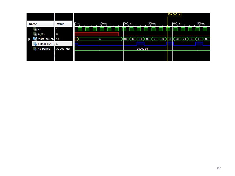
architecture behavioral of Exercise is
Begin process_counter: process(ck,a_res) is begin if (ck'event) and (ck='1') then if (a_res='1') then counter_status <= "00"; signal_out <= '0'; else counter_status <= counter_status + 1; if (counter_status = "10“ ) then signal_out<='1'; -- else signal_out <= '0'; end if; end process process_counter; end behavioral;
 is. begin. if (ck event) and (ck= 1 ) then. if (a_res= 1 ) then counter_status <= 00 ; signal_out <= 0 ; else. counter_status <= counter_status + 1; if (counter_status = 10 ) then signal_out<= 1 ; -- else signal_out <= 0 ; end if; end process process_counter; end behavioral;")
83
Module N counter with synchronous reset
Let’s design a modulo N programmable counter with synchronous reset A_RES and an ENABLE. The counter has an output END_COUNT activated when the count value is reeached library IEEE; use IEEE.STD_LOGIC_1164.ALL; use IEEE.STD_LOGIC_ARITH.ALL; use IEEE.STD_LOGIC_UNSIGNED.ALL; USE ieee.numeric_std.ALL; library UNISIM; use UNISIM.VComponents.all; entity Counter_module_N is Port (CK : in std_logic; A_RES : in std_logic; ENABLE : in std_logic; Max_val : in std_logic_vector (15 downto 0); -- Max_val -> N count COUNT : inout std_logic_vector (15 downto 0); END_COUNT : out std_logic); end Counter_module_N; architecture Behavioral of Counter_module_N is begin processo: process(CK, A_RES, ENABLE) if (CK='1') and (CK'event) then if (A_RES='1') then COUNT <= X"0000"; N.B. Hexadecimal notation !!! END_COUNT <= '0'; ; upon next clock elsif ENABLE='1' then Only if reset is inactive if COUNT < Max_val then COUNT <= COUNT Input value else COUNT <= X"0000"; end if; if COUNT = Max_val -1 then END_COUNT <= '1'; -- Upon next clock !!!! else END_COUNT <= '0'; end process processo; end Behavioral;
; -- Max_val -> N count. COUNT : inout std_logic_vector (15 downto 0); END_COUNT : out std_logic); end Counter_module_N; architecture Behavioral of Counter_module_N is. begin. processo: process(CK, A_RES, ENABLE) if (CK= 1 ) and (CK event) then. if (A_RES= 1 ) then. COUNT <= X 0000 ; -- N.B. Hexadecimal notation !!! END_COUNT <= 0 ; ; -- 0 upon next clock. elsif ENABLE= 1 then -- Only if reset is inactive. if COUNT < Max_val then COUNT <= COUNT Input value. else COUNT <= X 0000 ; end if; if COUNT = Max_val -1 then END_COUNT <= 1 ; -- Upon next clock !!!! else END_COUNT <= 0 ; end process processo; end Behavioral;")
84
Testbed internal signals
Testbench1/2 library IEEE; use IEEE.STD_LOGIC_1164.ALL; use IEEE.STD_LOGIC_ARITH.ALL; use IEEE.STD_LOGIC_UNSIGNED.ALL; USE ieee.numeric_std.ALL; library UNISIM; use UNISIM.VComponents.all; ENTITY Test IS END Test; ARCHITECTURE behavior OF Test IS COMPONENT Counter_modulo_N PORT( CK : IN std_logic; A_RES : IN std_logic; ENABLE : IN std_logic; Max_val : IN std_logic_vector(15 downto 0); COUNT : INOUT std_logic_vector(15 downto 0); END_COUNT : OUT std_logic ); END COMPONENT; signal CK : std_logic := '0'; signal A_RES : std_logic := '0'; signal ENABLE : std_logic := '0'; signal Max_val : std_logic_vector(15 downto 0) := (others => '0'); signal COUNT : std_logic_vector(15 downto 0); signal END_COUNT : std_logic; constant CK_period : time := 10 ns; BEGIN uut: Counter_modulo_N PORT MAP ( CK => CK, A_RES => A_RES, ENABLE => ENABLE, Max_val => Max_val, COUNT => COUNT, END_COUNT => END_COUNT ) Testbed internal signals
; COUNT : INOUT std_logic_vector(15 downto 0); END_COUNT : OUT std_logic. ); END COMPONENT; signal CK : std_logic := 0 ; signal A_RES : std_logic := 0 ; signal ENABLE : std_logic := 0 ; signal Max_val : std_logic_vector(15 downto 0) := (others => 0 ); signal COUNT : std_logic_vector(15 downto 0); signal END_COUNT : std_logic; constant CK_period : time := 10 ns; BEGIN. uut: Counter_modulo_N PORT MAP ( CK => CK, A_RES => A_RES, ENABLE => ENABLE, Max_val => Max_val, COUNT => COUNT, END_COUNT => END_COUNT. ) Testbed internal signals.")
85
Testbench 2/2 clock_process :process variable I: integer; begin
A_RES <= '1'; Max_val <= X"0007"; -- contare fino a 7 for I in 3 downto 0 loop ck <= '0'; wait for ck_period/2; ck <= '1'; end loop; A_RES <= '0'; ENABLE <= '1'; ENABLE <= '0'; for I in 1 downto 0 loop for I in 0 to 40 loop wait; end process; END;

86
In this simulation the counter basis is 7 and the notation is Hexadecimal

87
Array attributed Statement others
In VHDL there are also array attributes. For instance for a vector VECTOR: std_logic_vector(4 downto 0); VECTOR’length provides value 5 (like «sizeof» in C) Statement others With others it is possible to set the content of some or of all elements of a vector not otherwise explicitly set. For instance vector <= (0=>'1', others =>'0'); (the right arrow means always assignment). This statement set to 1 the LSbit and all others to 0 (How many ? With others it is not necessary to know this information).
; VECTOR’length provides value 5 (like «sizeof» in C) Statement others. With others it is possible to set the content of some or of all elements of a vector not otherwise explicitly set. For instance. vector <= (0=> 1 , others => 0 ); (the right arrow means always assignment). This statement set to 1 the LSbit and all others to 0 (How many With others it is not necessary to know this information).")
88
half_word = CONV_STD_LOGIC_VECTOR(value, 16);
Conversion functions In the IEEE libraries some functions are defined to convert values. For instance in the IEEE.std_logic_arith a function is defined to convert from integer to STD_LOGIC_VECTOR (and many others) <slv_sig> = CONV_STD_LOGIC_VECTOR(<int_sig>, <int_size>); For instance if half_word is a signal type STD_LOGIC_VECTOR(15 downto 0) and value is type integer, the conversion of value to a STD_LOGIC_VECTOR can be achieved through: half_word = CONV_STD_LOGIC_VECTOR(value, 16); In Xilinx ISE the functions are displayed when the toolbar icon is clicked. With the same command the precompiled components can be used. Integer with or withou sign Vettore Bits number
 <slv_sig> = CONV_STD_LOGIC_VECTOR(<int_sig>, <int_size>); For instance if half_word is a signal type STD_LOGIC_VECTOR(15 downto 0) and value is type integer, the conversion of value to a STD_LOGIC_VECTOR can be achieved through: half_word = CONV_STD_LOGIC_VECTOR(value, 16); In Xilinx ISE the functions are displayed when the toolbar icon is clicked. With the same command the precompiled components can be used. Integer with or withou sign. Vettore. Bits number.")
Similar presentations

>")


>")


